關(guān)鍵詞: FPGA , KC705 , Kintex-7 , Xilinx
Xilinx公司的7系列FPGA包括Artix™-7, Kintex™-7 和Virtex®-7 三個(gè)系列,具有超高端連接帶寬,邏輯容量和信號(hào)完整性,提供低成本,小型尺寸和大容量的要求最嚴(yán)格的高性能應(yīng)用.其中的Kintex-7 FPGA具有最高的性價(jià)比,其所組成的收發(fā)器從600 Mbps到最高的6.6 Gbps ,高達(dá)到28.05 Gbps,主要用在航空電子,LED背光的平板電視和3D TV,LTE基帶,手持超聲設(shè)備,多模式無(wú)線電,Prosumer數(shù)碼單反照相機(jī)和視頻IP網(wǎng)關(guān).本文介紹了7系列FPGA主要特性, Kintex-7 FPGA系列主要特性和應(yīng)用優(yōu)勢(shì),以及評(píng)估板KC705主要特性,方框圖, 評(píng)估板KC705主要元件, 配置電路圖,詳細(xì)電路圖和材料清單.
2012-2-7 12:35:46 上傳
Xilinx® 7 series FPGAs comprise three new FPGA families that address the complete range of system requirements, ranging from low cost, small form factor, cost-sensitive, high-volume applications to ultra high-end connectivity bandwidth, logic capacity, and signal processing capability for the most demanding high-performance applications. The 7 series devices are the programmable silicon foundation for Targeted Design Platforms that enable designers to focus on innovation from the outset of their development cycle. The 7 series FPGAs include:
• Artix™-7 Family: Optimized for lowest cost and power with small form-factor packaging for the highest volume applications.
• Kintex™-7 Family: Optimized for best price-performance with a 2X improvement compared to previous generation, enabling a new class of FPGAs.
• Virtex®-7 Family: Optimized for highest system performance and capacity with a 2X improvement in system performance. Highest capability devices enabled by stacked silicon interconnect (SSI) technology.
Built on a state-of-the-art, high-performance, low-power (HPL), 28 nm, high-k metal gate (HKMG) process technology, 7 series FPGAs enable an unparalleled increase in system performance with 2.9 Tb/s of I/O bandwidth, 2 million logic cell capacity, and 5.3 TMAC/s DSP, while consuming 50% less power than previous generation devices to offer a fully programmable alternative to ASSPs and ASICs. All 7 series devices share a unified fourthgeneration Advanced Silicon Modular Block (ASMBL™) column-based architecture that reduces system development and deployment time with simplified design portability.
7系列FPGA主要特性:
• Advanced high-performance FPGA logic based on real 6-input lookup table (LUT) technology configurable as distributed memory.
• 36 Kb dual-port block RAM with built-in FIFO logic for on-chip data buffering.
• High-performance SelectIO™ technology with support for DDR3 interfaces up to 1,866 Mb/s.
• High-speed serial connectivity with built-in multi-gigabit transceivers from 600 Mb/s to maximum rates of 6.6 Gb/s up to 28.05 Gb/s, offering a special low-power mode, optimized for chip-to-chip interfaces.
• A user configurable analog interface (XADC), incorporating dual 12-bit 1MSPS analog-to-digital converters with on-chip thermal and supply sensors.
• DSP slices with 25 x 18 multiplier, 48-bit accumulator, and pre-adder for high performance filtering, including optimized symmetric coefficient filtering.
• Powerful clock management tiles (CMT), combining phase-locked loop (PLL) and mixed-mode clock manager (MMCM) blocks for high precision and low jitter.
• Integrated block for PCI Express® (PCIe), for up to x8 Gen3 Endpoint and Root Port designs.
• Wide variety of configuration options, including support for commodity memories, 256-bit AES encryption with HMAC/SHA-256 authentication, and built-in SEU detection and correction.
• Low-cost, wire-bond, lidless flip-chip, and high signal integrity flipchip packaging offering easy migration between family members in the same package. All packages available in Pb-free and selected packages in Pb option.
• Designed for high performance and lowest power with 28 nm, HKMG, HPL process, 1.0V core voltage process technology and 0.9V core voltage option for even lower power.
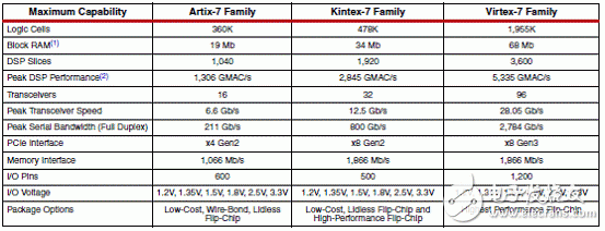
7系列FPGA特性比較表:
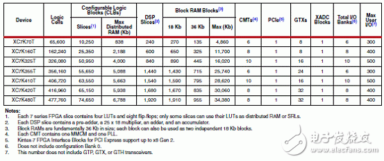
Kintex-7 FPGA系列主要特性:
2012-2-7 12:35:46 上傳
下載附件 (32.31 KB)Kintex-7 FPGA系列主要應(yīng)用和特點(diǎn):
Application
Description
Avionics
Kintex-7 FPGA price-performance drives SWAP-C benefits for aircraft video data bus systems.
LED Backlit Flat Panel Displays and 3DTV
Kintex-7 FPGA offers capabilities that enable flat panel display manufacturers to improve image quality, reduce power consumption, and reduce cost.
LTE Baseband
Meet stringent latency requirements and enable a common platform supporting Multiple Air Interface Standards such as LTE, WiMAX, and CDMA in a single component with Kintex-7 FPGA.
Portable Ultrasound
High I/O bandwidth and DSP processing power make Kintex-7 FPGAs highly effective for both front and back-end Ultrasound Processing.
Multi-mode Radio
Kintex-7 FPGAs help you to reduce cost and power consumption, deliver scalable platforms, and support multiple air interface standards.
Prosumer Digital SLR Cameras
Kintex-7 FPGA enables manufacturers of Prosumer Digital SLR cameras to implement control functions in auto-focus lenses and rapidly deploy enhancements in camera body controller/image processing ASICs.
Video over IP Gateway
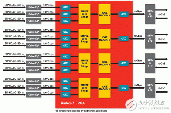
Reduce cost for Video over IP Gateways by integrating four 3:1, 3G-SDI-to-10GbE bridges in a single FPGA.
1. Kintex-7 FPGA系列在LTE通信應(yīng)用
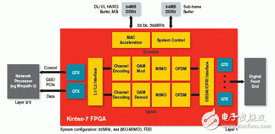
Kintex-7 FPGAs offer the best price-performance so designers can meet stringent latency requirements for LTE baseband processing in a common platform.
• Programmability enables a cost-effective common platform supporting multiple air interfaces such as LTE, WiMAX, and WCDMA
• Reduce total cost of ownership with the ability to scale and reuse designs from picocell to macrocell
• 3x capacity at the same cost of previous-generation FPGAs while consuming 40% less power
• Support for 9.8Gbps CPRI/OBSAI for high throughput
• Support for 6.144Gbps CPRI/OBSAI in a low-cost package option
2012-2-7 12:35:46 上傳
下載附件 (37.72 KB)圖1. Kintex-7 FPGA單片LTE通信基帶框圖(2x4MIMO)
2. Kintex-7 FPGA系列在醫(yī)療電子應(yīng)用
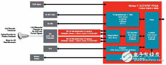
Support for 6.144Gbps CPRI/OBSAI in a low-cost package optionHigh I/O bandwidth and 144GMACS DSP processing power in chip-scale packaging make the Kintex-7 70T FPGA highly effective for both front- and back-end ultrasound processing. Designers can deploy a fully programmable 128-channel ultrasound implementation that scales up to 196 or 256 channels for high-end cart solutions or down to 64 or 32 channels for hand-held solutions.
• 128-channel implementation in a modular set of five Kintex-7 70T FPGAs offers 44% lower power, 45% lower cost, and 57% smaller form factor compared to previous-generation FPGAs
• Kintex-7 70T FPGAs offer 144GMACS from 240 DSP slices (288GMACS for symmetric filters)
• Built-in support for eight PCI Express Gen1/Gen2 channels enables high-bandwidth interface to host system
• Chip-scale packaging for small form factor
2012-2-7 12:35:46 上傳
下載附件 (30.4 KB)圖2. Kintex-7 FPGA系列在手持超聲設(shè)備的應(yīng)用框圖
3. Kintex-7 FPGA系列在廣播設(shè)備的應(yīng)用
Kintex-7 FPGAs enable cost-effective, low-power bridging of the serial digital interface (SDI) protocol onto IP technology for long-distance WAN transport to link local studios/live events, broadcast facilities, and satellite uplink stations using standard IP networks.
• Reduce power by 64% and reduce cost by 85% with a single XC7K160T FPGA implementation of a 12x 3G-SDI over 4x10GbE bridge compared to the equivalent function implemented in two Virtex-6 XC6L130T devices
• Reduce cost further with high-bandwidth interfaces that shrink BOM: 72-bit x 1,600Mbps DDR3 memory interface capability enables a single memory buffer that would require two or four memory buffers in previous-generation FPGAs
2012-2-7 12:35:46 上傳
下載附件 (63.44 KB)圖3. Kintex-7 FPGA系列在視頻IP網(wǎng)關(guān)的應(yīng)用框圖
Kintex-7 FPGA系列評(píng)估板KC705
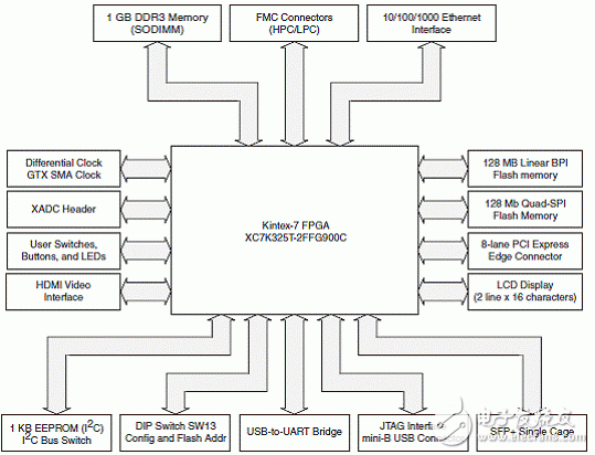
The KC705 evaluation board for the Kintex™-7 FPGA provides a hardware environment for developing and evaluating designs targeting the Kintex-7 XC7K325T-2FFG900C FPGA. The KC705 board provides features common to many embedded processing systems, including a DDR3 SODIMM memory, an 8-lane PCI Express® interface, a tri-mode Ethernet PHY, general purpose I/O, and a UART interface. Other features can be added by using mezzanine cards attached to either of two VITA-57 FPGA mezzanine connectors (FMC) provided on the board. High pin count (HPC) and low pin count (LPC) FMCs are provided.
評(píng)估板KC705主要特性:
• Kintex-7 XC7K325T-2FFG900C FPGA
• 1 GB DDR3 memory SODIMM
• 128 MB Linear BPI Flash memory
• 128 Mb Quad-SPI Flash memory
• Secure Digital (SD) connector
• USB JTAG via Digilent module
• Clock Generation
• Fixed 200 MHz LVDS oscillator (differential)
• I2C programmable LVDS oscillator (differential)
• SMA connectors (differential)
• SMA connectors for GTX transceiver clocking
• GTX transceivers
• FMC HPC connector (four GTX transceivers)
• FMC LPC connector (one GTX transceiver)
• SMA connectors (one pair each for TX, RX and REFCLK)
• PCI Express (eight lanes)
• Small form-factor pluggable plus (SFP+) connector
• Ethernet PHY SGMII interface (RJ-45 connector)
• PCI Express endpoint connectivity
• Gen1 8-lane (x8)
• Gen2 8-lane (x8)
• SFP+ Connector
• 10/100/1000 tri-speed Ethernet PHY
• USB-to-UART bridge
• HDMI codec
• I2C bus
• I2C MUX
• I2C EEPROM (1 KB)
• USER I2C programmable 3.3V LVDS oscillator
• DDR3 SODIMM socket
• HDMI codec
• FMC HPC connector
• FMC LPC connector
• SFP+ connector
• I2C programmable jitter-attenuating precision clock multiplier
• Status LEDs
• Ethernet status
• Power good
• FPGA INIT
• FPGA DONE
• User I/O
• USER LEDs (eight GPIO)
• User pushbuttons (five directional)
• CPU reset pushbutton
• User DIP switch (4-pole GPIO)
• User SMA GPIO connectors (one pair)
• LCD character display (16 characters x 2 lines)
• Switches
• Power on/off slide switch
• Configuration mode DIP switch
• VITA 57.1 FMC HPC Connector
• VITA 57.1 FMC LPC Connector
• Power management
• PMBus voltage and current monitoring via TI power controller
• XADC header
• Configuration options
• Linear BPI Flash memory
• Quad SPI
• USB JTAG configuration port
• Platform cable header JTAG configuration port
2012-2-7 12:35:46 上傳
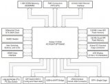
下載附件 (37.03 KB)圖4.評(píng)估板KC705方框圖
2012-2-7 12:35:46 上傳
下載附件 (58.03 KB)圖5.評(píng)估板KC705外形圖
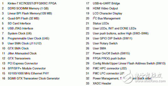
評(píng)估板KC705主要元件:
2012-2-7 12:35:46 上傳
下載附件 (27.55 KB)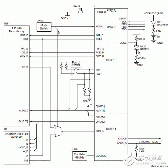
2012-2-7 12:35:46 上傳
下載附件 (31.57 KB)圖6.評(píng)估板KC705配置電路圖
KC705評(píng)估板詳細(xì)電路圖見(jiàn):
https://secure.xilinx.com/webreg/clickthrough.do?cid=181332&license=RefDesLicense&filename=kc705_Schematic_xtp132_rev1_0.pdf
KC705評(píng)估板材料清單見(jiàn):
https://secure.xilinx.com/webreg/clickthrough.do?cid=181320&license=RefDesLicense&filename=kc705_BOM_rdf0149_rev1_0.zip
詳情請(qǐng)見(jiàn):
ds180_7Series_Overview[1].pdf (563.87 KB, 下載次數(shù): 15)
2012-2-7 12:33:12 上傳
下載次數(shù): 15下載積分: 積分 -1 和
ug810_KC705_Eval_Bd[1].pdf (4.64 MB, 下載次數(shù): 81)
2012-2-7 12:34:36 上傳
下載次數(shù): 81下載積分: 積分 -1
 電子發(fā)燒友App




評(píng)論