關(guān)鍵詞: FPGA , VC707 , Virtex-7 , Xilinx
Xilinx公司的7系列FPGA產(chǎn)品包括Artix™-7系列, Kintex™-7系列和Virtex®-7系列,具有低成本,小尺寸,高性價比和大容量以及超高端連接帶寬,邏輯功能和信號處理能力等特性,適合要求最嚴(yán)格的高性能應(yīng)用.本文介紹了Xilinx 7系列FPGA主要特性,7系列三種FPGA性能比較表,以及Virtex-7 FPGA主要特性, Virtex-7 FPGA評估板VC707主要特性, 方框圖,電路圖和材料清單.
2012-4-1 14:52:47 上傳
Xilinx® 7 series FPGAs comprise three new FPGA families that address the complete range of system requirements, ranging from low cost, small form factor, cost-sensitive, high-volume applications to ultra high-end connectivity bandwidth, logic capacity, and signal processing capability for the most demanding high-performance applications. The 7 series devices are the programmable silicon foundation for Targeted Design Platforms that enable designers to focus on innovation from the outset of their development cycle. The 7 series FPGAs include:
• Artix™-7 Family: Optimized for lowest cost and power with small form-factor packaging for the highest volume applications.
• Kintex™-7 Family: Optimized for best price-performance with a 2X improvement compared to previous generation, enabling a new class of FPGAs.
• Virtex®-7 Family: Optimized for highest system performance and capacity with a 2X improvement in system performance. Highest capability devices enabled by stacked silicon interconnect (SSI) technology.
Built on a state-of-the-art, high-performance, low-power (HPL), 28 nm, high-k metal gate (HKMG) process technology, 7 series FPGAs enable an unparalleled increase in system performance with 2.9 Tb/s of I/O bandwidth, 2 million logic cell capacity, and 5.3 TMAC/s DSP, while consuming 50% less power than previous generation devices to offer a fully programmable alternative to ASSPs and ASICs. All 7 series devices share a scalable, optimized fourth-generation Advanced Silicon Modular Block (ASMBL™) column-based architecture that reduces system development and deployment time with simplified design portability.
Xilinx 7系列FPGA主要特性:
• Advanced high-performance FPGA logic based on real 6-input lookup table (LUT) technology configurable as distributed memory.
• 36 Kb dual-port block RAM with built-in FIFO logic for on-chip data buffering.
• High-performance SelectIO™ technology with support for DDR3 interfaces up to 1,866 Mb/s.
• High-speed serial connectivity with built-in multi-gigabit transceivers from 600 Mb/s to maximum rates of 6.6 Gb/s up to 28.05 Gb/s, offering a special low-power mode, optimized for chip-to-chip interfaces.
• A user configurable analog interface (XADC), incorporating dual 12-bit 1MSPS analog-to-digital converters with on-chip thermal and supply sensors.
• DSP slices with 25 x 18 multiplier, 48-bit accumulator, and pre-adder for high performance filtering, including optimized symmetric coefficient filtering.
• powerful clock management tiles (CMT), combining phase-locked loop (PLL) and mixed-mode clock manager (MMCM) blocks for high precision and low jitter.
• Integrated block for PCI Express® (PCIe), for up to x8 Gen3 Endpoint and Root Port designs.
• Wide variety of configuration options, including support for commodity memories, 256-bit AES encryption with HMAC/SHA-256 authentication, and built-in SEU detection and correction.
• Low-cost, wire-bond, lidless flip-chip, and high signal integrity flipchip packaging offering easy migration between family members in the same package. All packages available in Pb-free and selected packages in Pb option.
• Designed for high performance and lowest power with 28 nm, HKMG, HPL process, 1.0V core voltage process technology and 0.9V core voltage option for even lower power.
7系列比較表:
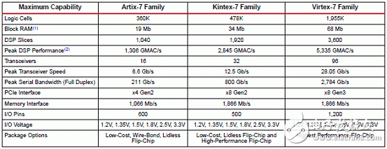
Virtex®-7 FPGAs are available in -3, -2, -1, and -2L speed grades, with -3 having the highest performance. The -2L devices can operate at either of two VCCINT voltages, 0.9V and 1.0V and are screened for lower maximum static power.
When operated at VCCINT = 1.0V, the speed specification of a -2L device is the same as the -2 speed grade. When operated at VCCINT = 0.9V, the -2L performance and static and dynamic power is reduced. The -2G speed grade is available in devices utilizing Stacked Silicon Interconnect Technology. The -2G speed grade supports 12.5 Gb/s GTX,13.1 Gb/s GTH, and 28.05 Gb/s GTZ transceivers as well as the standard -2 speed grade specifications.
Virtex-7 FPGA DC and AC characteristics are specified for commercial, extended, and industrial temperature ranges.
Except the operating temperature range or unless otherwise noted, all the DC and AC electrical parameters are the same for a particular speed grade (that is, the timing characteristics of a -1 speed grade industrial device are the same as for a -1 speed grade commercial device). However, only selected speed grades and/or devices are available in
each temperature range.
All supply voltage and junction temperature specifications are representative of worst-case conditions. The parameters included are common to popular designs and typical applications.
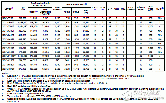
Virtex-7 FPGA主要特性:
2012-4-1 14:52:47 上傳
下載附件 (45.3 KB)Virtex-7 FPGA評估板VC707
The VC707 evaluation board for the Virtex®-7 FPGA provides a hardware environment for developing and evaluating designs targeting the Virtex-7 XC7VX485T-2FFG1761C FPGA. The VC707 board provides features common to many embedded processing systems, including a DDR3 SODIMM memory, an 8-lane PCI Express® interface, a tri-mode Ethernet PHY, general purpose I/O, and two UART interfaces. Other features can be added by using mezzanine cards attached to either of two VITA-57 FPGA mezzanine connectors (FMC) provided on the board. Two high pin count (HPC) FMCs are provided.
評估板VC707主要特性:
•Virtex-7 XC7VX485T-2FFG1761C FPGA
•1 GB DDR3 memory SODIMM
•128 MB Linear BPI Flash memory
•USB 2.0 ULPI Transceiver
•Secure Digital (SD) connector
•USB JTAG via Digilent module
•Clock Generation
•Fixed 200 MHz LVDS oscillator (differential)
•I2C programmable LVDS oscillator (differential)
•SMA connectors (differential)
•SMA connectors for GTX transceiver clocking
•GTX transceivers
•FMC1 HPC connector (eight GTX transceivers)
•FMC2 HPC connector (eight GTX transceiver)
•SMA connectors (one pair each for TX, RX and REFCLK)
•pCI Express (eight lanes)
•Small form-factor pluggable plus (SFP+) connector
•Ethernet PHY SGMII interface (RJ-45 connector)
•pCI Express endpoint connectivity
•Gen1 8-lane (x8)
•Gen2 8-lane (x8)
•SFP+ Connector
•10/100/1000 tri-speed Ethernet PHY
•USB-to-UART bridge
•HDMI codec
•I2C bus
•I2C MUX
•I2C EEPROM (1 KB)
•USER I2C programmable LVDS oscillator
•DDR3 SODIMM socket
•HDMI codec
•FMC1 HPC connector
•FMC2 HPC connector
•SFP+ connector
•I2C programmable jitter-attenuating precision clock multiplier
•Status LEDs
•Ethernet status
•power good
•FPGA INIT
•FPGA DONE
•User I/O
•USER LEDs (eight GPIO)
•User pushbuttons (five directional)
•CPU reset pushbutton
•User DIP switch (8-pole GPIO)
•User SMA GPIO connectors (one pair)
•LCD character display (16 characters x 2 lines)
•• Switches
•power on/off slide switch
•Configuration mode DIP switch
•VITA 57.1 FMC1 HPC Connector
•VITA 57.1 FMC2 HPC Connector
•power management
•pMBus voltage and current monitoring via TI power controller
•XADC header
•Configuration options
•Linear BPI Flash memory
•USB JTAG configuration port
•platform cable header JTAG configuration port
2012-4-1 14:52:47 上傳
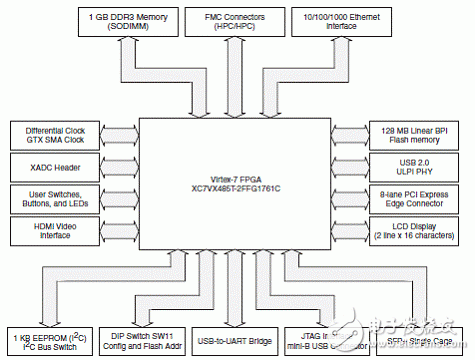
下載附件 (30.79 KB)圖1.評估板VC707方框圖
2012-4-1 14:52:47 上傳
下載附件 (92.13 KB)圖2.評估板VC707外形圖和元件分布圖
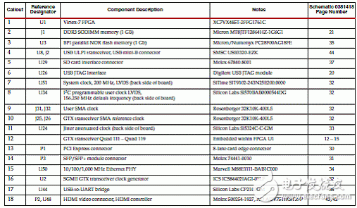
評估板VC707元件分布表:
2012-4-1 14:52:47 上傳
下載附件 (34.21 KB)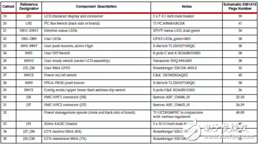
2012-4-1 14:52:47 上傳
下載附件 (36.03 KB)VC707評估板電路圖見:
https://secure.xilinx.com/webreg/clickthrough.do?cid=181656&license=RefDesLicense&filename=vc707_Schematic_xtp135_rev1_0.pdf
VC707評估板材料清單見:
https://secure.xilinx.com/webreg/clickthrough.do?cid=181642&license=RefDesLicense&filename=vc707_BOM_rdf0154_rev1_0.zip
詳情請見:
ds183_Virtex_7_Data_Sheet[1].pdf (1.53 MB, 下載次數(shù): 25)
2012-4-1 14:49:37 上傳
下載次數(shù): 25下載積分: 積分 -1 和
ug885_VC707_Eval_Bd.pdf (7.06 MB, 下載次數(shù): 23)
2012-4-3 06:52:38 上傳
下載次數(shù): 23下載積分: 積分 -1
 電子發(fā)燒友App


評論