Resistive Element Sensors and the Four DAC Compensation Architecture
Resistive element sensors, most notably the Wheatstone bridge configured piezo resistive devices, have dominated the low- to medium-accuracy pressure sensing industry since the early 1980s.The principal source of measurement error with these devices is changing sensitivity and output offset with temperature. Signal conditioning and calibration provide greater accuracy and lower cost. One of the most effective solutions to this basic requirement is the analog path conditioning architecture using four digital-to-analog converters (DACs) to provide the necessary temperature corrections.
The temperature sensitivity in the gain for piezo resistive sensors stems from thermal coefficient of sensitivity (TCS) and the thermal coefficient of resistance (TCR). TCS effects arise from dimensional and stiffness changes in the sensor over temperature. TCS is always negative (sensitivity reducing with increasing temperature). TCR describes the change in sensor bridge resistance with temperature and is normally positive.
Most resistive element sensors are designed to make best use of the opposing signs of these two thermal coefficients. The aim is to produce a sensor with TCS slightly lower in magnitude than TCR. This results in a sensor which, when driven from a constant current source, exhibits a much reduced total temperature sensitivity and allows external temperature compensation to be easily applied. The resulting condition is portrayed in the graph of Figure 1, which contains normalized temperature responses for bridge resistance (Rb) and pressure sensitivity. The slopes of these two responses represent the TCR and TCS characteristics of the sensor. The third curve in Figure 1 represents the ideal response of sensor bridge voltage (Vb) required to balance the sensitivity curve and produce a sensor with a null temperature coefficient of gain.
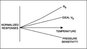
Figure 1. Normalized responses of sensor bridge resistance and pressure sensitivity.
The first task of a conditioning circuit, which acts on the bridge drive current, is to produce the ideal Vb curve shown in Figure 1. The second conditioning requirement is to produce a signal which balances the sensor's output offset behavior. Resistive bridge sensors typically exhibit output offset behavior that can be described in terms of a fixed component plus a temperature dependent component. Both of these components can be corrected by summing offsets into the signal path. One of these offset components should have a fixed value while the second should have a temperature characteristic, which opposes that of the sensor offset temperature dependent component. An analog path, four DAC system, which satisfies these requirements is shown in Figure 2.
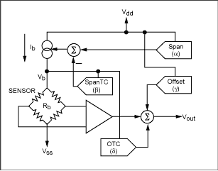
Figure 2. System of digital to analog converters for temperature compensation of resistive element sensors, as found in the MAX1452 and similar devices.
In the system illustrated in Figure 2, the Span DAC and SpanTC DAC combine to provide the necessary modification to the bridge voltage Vb. The Span DAC takes it's reference from the positive supply rail VDD and thus provides an output that is ratio-metric to VDD and independent of temperature. The SpanTC DAC is referred to the bridge voltage Vb and thus has an output that is temperature dependent (since Vb is temperature dependent). The resulting bridge voltage response characteristic is then of the form given in Equation 1.

Where:
Span = Span DAC value, range 0 to 1
SpanTC = SpanTC DAC value, range 0 to 1
K1 = arbitrary constant
K3 = arbitrary constant
Rb = sensor bridge resistance
VDD = conditioner IC supply voltage
Compensation for the sensor output offset characteristic is provided by the Offset DAC and OTC DAC. As with the Span and SpanTC DACs, the offset correction DACs are arranged to provide both fixed (referenced to VDD) and temperature dependent (referenced to bridge voltage) outputs. The Offset and OTC DACs provide outputs that are a positive or negative fraction of their reference voltages. The modification to the output of the system of Figure 2, provided by these offset correcting DACs, is then of the form shown in Equation 2.
Where:
Offset = Offset DAC value, range 0 to ±1
OTC = OffsetTC DAC value, range 0 to ±1
K2 = arbitrary constant
K4 = arbitrary constant
Rb = sensor bridge resistance
Vb = sensor bridge voltage
VDD = conditioner IC supply voltage
Implementing a First-Order Calibration using the Conditioning Architecture of Figure 2
Using the four DAC architecture, virtually any piezo resistive bridge pressure sensor can be calibrated, to a first-order fit, over the entire operating temperature range. The objective of a first-order, fixed value, calibration is to find unique calibration values for each of the four DACs in the compensation system. These are the values required to produce the desired bridge voltage response of Figure 1, and to correct for the sensor offset response. This is achieved with a simple two temperature, two pressure calibration.Span Compensation
The first part of the calibration process deals with span compensation of the sensor and is concerned with modifying the sensor bridge voltage response. The method employed requires an ideal value of bridge voltage to be determined at each temperature. Pairs of values for the Span and SpanTC DACs, and the corresponding value for bridge voltage, are then found at each temperature. The bridge voltage values generated should be close to the ideal bridge voltage value at the current temperature. Exactly matching values for Vb at each temperature should be avoided. This is because the mathematical solution to the resulting set of equations is in matrix form and will generate a singular matrix in the event that identical values for Vb are used.The process starts at the first calibration temperature (T1) by loading the Span and SpanTC DAC registers with nominal values and measuring the bridge voltage and conditioner IC output span. The value of bridge voltage required at this temperature may be calculated by the expression given in Equation 3.
Three values for the SpanTC DAC (β11, β12, β13) are then chosen and loaded, in turn, to the SpanTC DAC register. For each of these SpanTC DAC settings a corresponding value for Span
DAC (α) is determined that produces a bridge voltage approximately equal to the required Vb value.
Having completed the measurements at T1, the test chamber temperature is then changed to the second calibration temperature (T2) and the process is repeated. Figure 3 illustrates this process and the measurements required at each temperature.
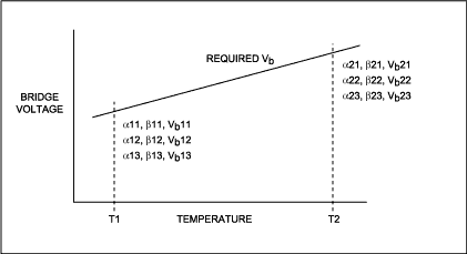
Figure 3. DAC settings and measurements required during a first-order, fixed value, span calibration.
The Span calibration process is completed by calculating the required values for Span (α) and SpanTC (β) and loading these to the respective signal conditioner registers. The calculations required are given in Figure 4.
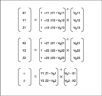
Figure 4. Matrix calculations required to determine values for Span and SpanTC. X1, X2, Y1, Y2, Z1 and Z2 are intermediary coefficients.
Offset Compensation
Figure 5 shows the full, first-order, calibration measurement system using four DACs. The measurements shown in brackets in Figure 5 are those required to perform the offset compensation for the sensor. While at temperature T1 and with minimum pressure applied to the sensor the Offset DAC is adjusted to produce an output voltage approximately equal to the desired zero output. The OTC DAC is normally set to zero during this phase of the calibration. Following Offset DAC adjustment, the values of Offset DAC (γ1), OTC DAC (δ1), output voltage (VOUT1) and bridge voltage (Vb1) are recorded for later use.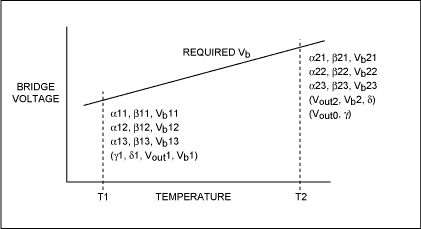
Figure 5. DAC settings and measurements required for a full first-order, fixed value, calibration.
Following completion of the span calibration, while at temperature T2 and with minimum pressure applied to the sensor, the Offset and OTC DAC registers are loaded with the values γ1 and δ1 recorded at T1. The resulting value of output voltage (VOUT2), and the current value for bridge voltage (Vb2) are measured and recorded. The OTC DAC is then adjusted to produce the output voltage value given by Equation 4.
The offset calibration is completed by adjusting the Offset DAC to produce an output equal to the desired 'zero' output level.
Use of a Look-Up Table to Simplify the Calibration Process
The inclusion of a temperature driven look-up table in the signal conditioning architecture adds a great deal of flexibility to the system and can simplify the calibration process substantially. Only two DACs are needed for a basic look-up table driven system, one for span and one for offset. A basic look-up table based compensation system is illustrated in Figure 6. One advantage of this type of system is calibration speed.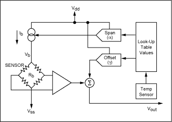
Figure 6. System of two digital to analog converters with look-up table, as typified by devices such as the MAX1452 and MAX1455.
For a first-order temperature compensation the calibration process employed with a look-up table based system is similar to that described for the four DAC, fixed value, calibration. As with the fixed value system, two calibration temperatures are required. At each temperature the ideal value for sensor bridge voltage is determined using the expression of Equation 3. A value for Span DAC (α) is then found which produces the required bridge voltage value. The Span DAC value thus determined is the required look-up table value at that temperature. The Offset DAC look-up table value (γ) required is that which, with minimum pressure applied to the sensor, produces the desired output 'zero' reading. Figure 7 illustrates this process and the measurements required at each temperature.
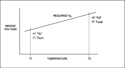
Figure 7. DAC settings and measurements required during first-order, look-up table, calibration.
The first-order calibration is then completed by loading the look-up tables for Span DAC and Offset DAC with values obtained from a linear interpolation between the values recorded for each DAC at each temperature.
Comparison of Calibration Schemes
So far two calibration schemes have been discussed. These being fixed value and look-up table derived. The strengths and weaknesses of these can be analyzed in terms of system error conditions and calibration efficiency. Both of the schemes described provide first -order compensation for temperature related errors. The accuracy of the compensation scheme then has a dependence on the accuracy of the compensation temperature measurement. In the fixed value calibration, all of the temperature information was derived from the sensor bridge resistance. This system should therefore minimize any errors that may be produced by transient thermal conditions.With the look-up table system calibration, the temperature information is typically derived from an on chip temperature sensor which is used to drive the look-up table pointer. Any temperature differences that exist between the sensor and the conditioning IC will therefore give rise to errors in the sensor compensation by pointing to adjacent locations in the look-up table.
An additional source of error for a first-order calibration is any second-order, or higher, terms in the sensor temperature response. The fixed value calibration scheme may only be applied as a first-order compensation and cannot correct for higher-order effects in the temperature response curve. The look-up table compensation may be applied at as many temperature intervals as required, allowing for virtually any order of temperature curve to be accommodated.
A further consideration is the time required to complete a sensor calibration. Calibration throughput is largely a function of temperature and pressure settling times and the time taken to determine and program the compensation coefficients for each sensor. With small volume production the settling times tend to dominate the calibration time. With high volume production the time required for the measurements on each sensor becomes more significant. It may only take one or two seconds to perform a single measurement set at one temperature. The fixed value calibration scheme requires nine such measurement sets for a full, first-order, calibration while the look-up table system requires only four.
Look-Up Table Calibration with Generic SpanTC DAC Value
It is possible to tailor the calibration scheme, using a combination of aspects from the fixed value and look-up table calibrations, to provide an optimum compromise between sensor accuracy under transient temperature conditions and calibration speed. One such scheme utilizes the offset correction method from the fixed value calibration, together with a generic value for the SpanTC DAC, while retaining most of the speed of the look-up table based calibration.In the look-up table calibration scheme previously described the SpanTC DAC was not considered to be part of the calibration system and was set to a nominal value. For any sensor there will be a unique value for SpanTC that perfectly compensates the sensor's thermal gain response at any two temperature points. This is the value that would have been determined by the application of the fixed value calibration method. Had the SpanTC register been set to this value at the start of a look-up table calibration, then the values determined for Span DAC would have been the same at both measurement temperatures. Under this condition all of the span related temperature information would be derived from the sensor bridge resistance. Equally, had the SpanTC register been loaded with a generic value, close to the actual value required, then there would be only a small difference between the Span DAC values at the two temperatures. This would produce a system in which most of the temperature information would be bridge resistance derived and which would be relatively insensitive to thermal transients.
A statistical analysis of sensor calibration data will yield an average SpanTC DAC value that can be used as the generic value for a particular sensor type. Ideally, the data used for this should be the actual SpanTC DAC values recorded from a suitable number of sensor calibrations. Further, having calculated the distribution of values for SpanTC, it is possible to predict the error distribution of the calibrated sensors as a function of any temperature difference that may exist between the sensor and the conditioning IC. The precise formula for this error prediction will depend on the conditioning architecture employed. The expression given in equation 5 has been determined for the MAX1452* signal conditioning IC and may be used to calculate the errors produced by the use of a non-ideal (generic) SpanTC value as a function of the temperature difference between the sensor and conditioning IC.
*The MAX1452 signal conditioning IC from Maxim Integrated Products is a good example of the current generation of conditioning products and features a four DAC architecture together with a fine pitched temperature driven look-up table. Figure 8 shows a schematic of the MAX1452.

Where:
ΔT = temperature difference between sensor and conditioning IC
KR = temperature coefficient of bridge resistance (Ω/°C)
β0= required SpanTC DAC value, range 0 to 1
β1= actual (generic) SpanTC DAC value, range 0 to 1
Rb = sensor bridge resistance
RSTC = setting resistor value associated with the SpanTC DAC
N = current multiplier gain (value internally set within conditioner IC)
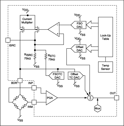
Figure 8. MAX1452 sensor conditioner I.C.
Sensor offset behavior does not lend itself to the programming of generic DAC values. This is because the offset could be either positive or negative. The preferred solution for offset compensation is therefore to use the system provided by the fixed value calibration method.
The resulting calibration technique, which uses a look-up table for Span DAC together with a generic value for SpanTC and fixed value calibration method for Offset and OTC, is illustrated in Figure 9.
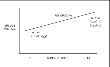
Figure 9. DAC settings and measurements required for a first-order look-up table compensation with generic SpanTC value and fixed value offset determination method.
The first-order calibration is then completed by loading the Span DAC look-up table with interpolated values and the Offset (table) and OTC (register) with figures calculated using the fixed value calibration offset technique. The result is a solution which retains much of the calibration speed advantage of the look-up table based system, but which exhibits substantially reduced susceptibility to thermal transient errors.
Higher-Order, Look-Up Table, Schemes Augmented by a Fixed Value Calibration
In addition to the obvious advantages in calibration throughput, the look-up table architecture has the capability to accommodate virtually any order of temperature response. This is most easily achieved by providing additional temperature points in the look-up table calibration previously described. If thermal transient errors are of concern then an extension of the generic SpanTC value method can be used or, for ultimate accuracy, a true combination of the fixed value and look-up table calibrations can be applied.By way of example, a second-order temperature compensation could be performed by applying a, first-order, fixed value calibration at two temperatures and then using the normal look-up table method for the third temperature. Higher-order temperature calibrations would be accommodated by simply adding further temperature points using the look-up table method. The fixed value calibration at the first two temperatures is used to determine the values for the SpanTC and OTC DACs. Typical temperatures for a three-point calibration would be minimum, ambient and maximum. The best results are normally obtained if the first two temperatures are the minimum and maximum, but for convenience it is often desirable to use ambient as the first temperature. Figure 10 illustrates this method for temperature measurements in the sequence: ambient temperature, minimum temperature, maximum temperature.
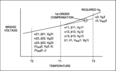
Figure 10. DAC settings and measurements required for combination calibration: first-order, fixed value, plus second-order look-up table compensation.
The required SpanTC and OTC DAC values are calculated and programmed following measurements at T2. Similarly, the values of Span and Offset are found, and recorded. These values are valid at both T1 and T2. At the third, and any subsequent, temperatures only the values for Span and Offset need be determined. The calibration is completed by the application of a suitable polynomial fit to the Span and Offset data and subsequent loading of the look-up tables.
A Versatile Sensor Signal Conditioning Solution
The versatility of a look-up table based, four DAC, analog path conditioning system is undeniable. With a variety of sensor calibration schemes supported, an optimum mix of accuracy and speed is readily available for most applications. Four such schemes have been described in the preceding text, each addressing particular temperature performance and calibration throughput requirements. Variations of these may readily be found, and optimized to meet particular requirements.
 電子發(fā)燒友App














評論