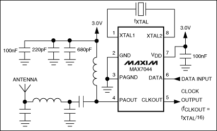
The MAX1472, MAX1479, and MAX7044 300MHz to 450MHz ASK transmitter ICs are used in applications that require extremely small packages, such as automobile key fobs and tire-pressure monitors. Quite often, a small loop is the only antenna that will fit into one of these packages. Because loops are very small compared to the wavelength at these frequencies, they are extremely high-Q and present a challenge to good impedance matching.
This application note shows the typical impedance values for small loops and suggests matching networks for these impedances. It demonstrates the effectiveness of these networks in suppressing harmonics of the transmitted frequency. Most transmitter ICs that serve these applications, like the Maxim MAX7044, MAX1472, and MAX1479, are biased for maximum efficiency rather than maximum linearity, which means that the harmonic content of the power amplifier (PA) output may be very high. Regulatory agencies in all countries where these devices are used restrict spurious emissions, so attenuating harmonic power from the PA is very important.
A complete model for the impedance match of a loop to the Maxim transmitter ICs must include the bias inductor, the output capacitance of the PA, traces, package, parasitics, etc. These factors will slightly modify the matching component values defined in this note. The networks detailed here match the MAX7044 transmitter, but also work satisfactorily with the MAX1472 and MAX1479. The MAX7044 achieves its highest efficiency when driving a 125ohm load, while the MAX1472 and MAX1479 favor a load of roughly 250ohms. Using the MAX1472 and MAX1479 with these networks increases mismatch loss by about 1dB?the networks can be slightly altered to recover this loss if desired.
Impedance of an Electrically Small-Loop Antenna
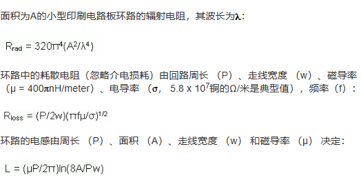
The radiation resistance of a small, printed circuit-board loop with area A at a frequency whose wavelength is is given by:

The dissipative resistance in the loop, ignoring dielectric loss, is calculated by the loop perimeter (P), the trace width (w), the magnetic permeability (µ = 400 nH/meter), the conductivity (, 5.8x10⁷ ohms/meter for copper is typical), and the frequency (f):

The loop's inductance is determined by the perimeter (P), the area (A), the trace width (w), and the magnetic permeability (µ):

These three quantities are derived from expressions in antenna theory textbooks.1,2
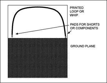
A typical printed circuit-board loop, from which dimensions are used to calculate representative resistive and reactive values for a small loop, is shown in the drawing of Figure 1. It is roughly rectangular, 25mm by 32mm, with a trace width of 0.9mm. At 315MHz, these dimensions lead to the following values for the three quantities listed above:

For the other commonly used frequency of 433.92MHz, the values are:


Figure 1. Small Loop on a Printed Circuit Board
The radiation resistance is extremely small. In addition, the resistance arising from the dissipative losses can be more than ten times the radiation resistance, which means that the best radiation efficiency possible with this loop is about 8% at 315MHz and 27% at 433.92MHz.The matching network must minimize mismatch losses and additional dissipative losses from the matching components. Typically, a small loop may be able to radiate only a few percent of the power that comes from the transmitter.
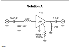
Basic Matching Network
The simplest matching network is the "split capacitor," described in a recent Microwaves & RF article.3 Connecting this network to the PA output with the bias inductor, as shown in Figure 2 below, makes it possible to adjust the value of C2 so that it resonates with the parallel combination of L1, the PA-related capacitance, and the residual reactance from C1 and the loop-antenna inductance. The equivalent series resistance (ESR) of the capacitor C1 is typically 0.138ohms, so the total resistance of the small loop with the series capacitor is 0.46ohms at 315MHz.
At the resonant-matching network frequency of 315MHz, the tiny loop resistance is transformed by the series reactance of the loop and C1 to an equivalent parallel circuit with the optimum load resistance of 125ohms (best load impedance for maximum MAX7044 efficiency). Notice that the efficiencies quoted in the MAX7044 data sheet are for a 50ohm load. The optimum resistance for radiated efficiency may not be the same. Our PAs maintain high efficiency across a broad range of impedances and power levels. The parallel capacitance, C2, and the parallel inductance of the bias inductor, L1, tune out the reactance of the equivalent parallel circuit.

Figure 2. Split Capacitor with Bias Inductor
The combination of C1 and the loop inductance form a positive reactance at the frequency of interest. Consequently, we can consider the two capacitors and loop inductance as an "L" matching network (shunt C, series L) that transforms the small loop resistance up to 125ohms. Looking from left to right, it is a lowpass high- to low-matching network. One could argue that the bias inductor is not essential to matching. However, the bias inductor actually helps reject higher harmonics and is essential for providing a DC path for the PA's operating current.
Table 1 shows the values that give a perfect match for the loop antenna described above.
Table 1. Ideal Component Values for Split Capacitor Match
| At 315MHz | At 433.92MHz |
| C1= 2.82pf | C1 = 1.47pf |
| C2= 63pf | C2 = 43pf |
| L1= 36nH | L1 = 27nH |
The C2 capacitance in the table does not include approximately 2pf that comes from the PA output and PC-board stray capacitance. This 2pf was added to the C2 values in all the matching calculations presented in this note.
The frequency dependence of this match at 315MHz is shown in the RF power transfer curves of Figure 3. These curves were computed by evaluating the expression for the power delivered from a source (RS) to a load impedance (RL + XL), where the load impedance is the loop antenna impedance transformed by the matching network:

This expression was multiplied by the antenna efficiency and the power loss arising from the matching components to get the total ratio of power radiated to power available.
All plots are shown at 315MHz and discussion of frequency dependence applies only to 315MHz.The behavior at 433.92MHz is similar, but not shown.
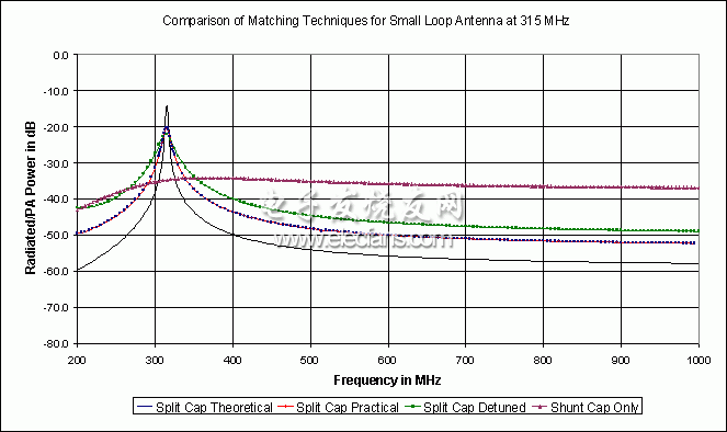
Figure 3. Power Transfer from RFIC Transmitter to Loop Antenna
Assuming that the model for the loop antenna is correct and that exact values of the matching capacitors are realized, the mismatch loss is 0dB; the antenna loss of -14.1dB is just the efficiency loss and dissipative loss added by the capacitors (radiation resistance divided by total resistance). This match is a vast improvement over the 36.2dB loss with no match at all (25dB mismatch loss, plus 11.2dB efficiency loss) and the 34.7dB loss from a single shunt capacitance that tunes out the antenna reactance (19dB mismatch loss, plus 15.7dB efficiency and capacitor dissipative loss). The power transfer for the single shunt-capacitor "match" is included in the plots as a reference.
In practice, the small-loop antenna has a much lower Q than theory predicts. Calculations made from laboratory measurements of the printed circuit-board loop of Figure 1 yield a total equivalent-series resistance of 2.2ohms at 315MHz instead of the theoretical 0.46ohms. Using this resistance, the standard capacitor and inductor values that match the loop are given in Table 2.
Table 2. Practical Component Values for Split-Capacitor Match
| At 315MHz | At 433.92MHz |
| C1= 3.0pf | C1 = 1.5pf |
| C2= 33pf | C2 = 27pf |
| L1= 27nH | L1 = 20nH |
The power transfer for the practical loop antenna is also shown in Figure 3. Because the loss resistance of the practical loop is roughly four times higher than the theoretical loop, the best power transfer is about -20dB instead of -14dB. Although the power-transfer curve is wider in frequency than the theoretical loop, it is still narrow enough for component tolerances to move the peak to another frequency and reduce the power transfer at the intended frequency. If all three matching components are 5% high in value, the power transfer drops to -26dB.
The power transfer characteristic can be widened in frequency, and hence made less sensitive to component tolerances, by "detuning" the matching network. This can be done by the "brute force" method: simply adding resistance to the loop antenna, or transforming the impedance to a value that is not perfectly matched to the transmitter. With either approach, the matching bandwidth is broadened at the expense of either higher power dissipation in the added resistor, or higher mismatch loss in the detuned matching network. Taking some power loss in return for having a predictable power transfer may be preferable, because the penalty for drifting off frequency in a narrowband match is so high.
The broadening approach used here matches the loop antenna to a higher impedance than is intended for the MAX7044 (500 ohms to 1000ohms instead of 125ohms), and accepts the mismatch loss (along with the unavoidable dissipative losses). This approach reduces the operating current as an added benefit.
Table 3 shows a set of Ls and Cs that transform the loop impedance to about 500ohms. They are rounded to the nearest standard L and C values.
Table 3. Component Values for a Wider Bandwidth Split-Capacitor Match
| At 315MHz | At 433.92MHz |
| C1= 3.3pf | C1 = 1.65pf (2pf x 3.3pf in series) |
| C2= 22pf | C2 = 15pf |
| L1= 27nH | L2 = 20nH |
This circuit decreases the power transfer at 315MHz to -22dB, but reduces the variation in loss with a 5% component tolerance to 3dB.
Figure 3 shows the losses in the tuning networks discussed above. Notice how narrow the perfectly tuned networks are, and how the "detuned" networks have more loss but are wider in bandwidth.
How well do these simple split-capacitor networks reject harmonics? Figure 3, which extends to 1000MHz, shows that the theoretical match-frequency response is down by 56dB at the second harmonic and 58dB at the third harmonic. Because the response is down by 14dB at the fundamental frequency, its second and third harmonic rejection is 42dB and 44dB, respectively. Because the practical and "detuned" matches are much more typical, they are the real indicators of harmonic rejection. The practical match is down 20dB at the fundamental and 50dB at the second harmonic, so the second harmonic rejection is 28dB. The "detuned" match is down 22dB at the fundamental and 46dB at the second harmonic, so the second harmonic rejection is 24dB. This rejection is not adequate for radiating the maximum average power possible allowed by the FCC at 315MHz. The allowable, radiated field strength of about 6000µV/m corresponds to radiated power of -19.6dBm. The second harmonic cannot exceed 200µV/m (-49dBm), so almost 30dB of harmonic rejection is needed for a transmitter to radiate the maximum allowable average power. FCC regulations for the 260MHz to 470MHz unlicensed band permit low-duty-cycle, peak-power radiation at levels as much as 20dB above the average power. Consequently, there are situations where even more than 30dB of second harmonic rejection is needed.
Matching Network with Higher Carrier Harmonic Rejection
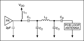
One simple way to achieve better harmonic rejection is to add a lowpass filter to the matching network. This can be done with a pi network inserted between the split capacitor-matching network and the transmitter output. Because the pi network can transform impedances, there are many possible combinations of impedance transformations. The examples here yield realistic values of L and C matching components. Figure 4 shows the network: one parallel capacitor in the lowpass filter has been combined with the parallel capacitor in the split-C matching network; the other parallel capacitor's value has been adjusted to tune out the bias inductor and the stray capacitances in the IC, in addition to serving as part of the matching network.
The values that give a nearly perfect match for the loop antenna in Figure 4 are shown in Table 4 below.
Table 4. Component Values for a Split-Capacitor Match with Improved Harmonic Rejection
| At 315MHz | At 433.92MHz |
| C1 = 3.0pf | C1 = 1.5pf |
| C2 = 33pf | C2 = 30pf |
| C3 = 12pf | C3 = 8.2pf |
| L1 = 51nH | L1 = 33nH |
| L2 = 47nH | L2 = 33nH |

Figure 4. Split-C Matching Network Combined with a Lowpass Filter
In Figure 4's configuration, the split C transforms the low loop resistance to roughly 150ohms (very close to the 125ohms for maximum efficiency of the PA) and the pi network is a lowpass filter designed for 125ohms input and output impedance. The mismatch loss is -0.1dB, and the bandwidth of this match is once again narrow and highly sensitive to component tolerances. The match is still very narrow because an exact impedance match was attempted, although with more than one network. The result is still the same: a narrow bandwidth match that is sensitive to component tolerances.
The bandwidth of this matching network can be increased (and the sensitivity-to-component tolerances decreased) by detuning the split-capacitor matching network, but retaining the 12ohm pi-network lowpass filter. The C1 and C2 values shown in the table below transform the parallel resistance of the loop antenna to about 500ohms instead of the 150ohms in the best match. The resulting mismatch between the antenna and the 125ohm lowpass filter increases the mismatch loss to 2dB but broadens the matching bandwidth.
The values for this match are given in Table 5.
Table 5. Component Values for a Wider Bandwidth Split-Capacitor Match with Improved Harmonic Rejection
| For 315MHz | For 433.92MHz |
| C1 = 3.3pf | C1 = 1.65pf |
| C2 = 22pf | C2 = 18pf |
| C3 = 12pf | C3 = 8.2pf |
| L1 = 51nH | L1 = 33nH |
| L2 = 47nH | L2 = 33nH |
Consequently, the output of the split-capacitor match is intentionally mismatched to the pi section. Changing the split-capacitor values to raise the transformed loop resistance higher than 500ohms while maintaining the same pi-matching network, further widens the matching bandwidth with the attendant increase in mismatch loss.
The behavior of the near-ideal matching network and the de-tuned network, along with a simple shunt capacitor for reference, is shown in Figure 5. While these data are similar to the plots in Figure 3, the harmonic rejection is quite different. The near-ideal match now has 49dB of second harmonic rejection, and the de-tuned match has 44dB of second harmonic rejection.
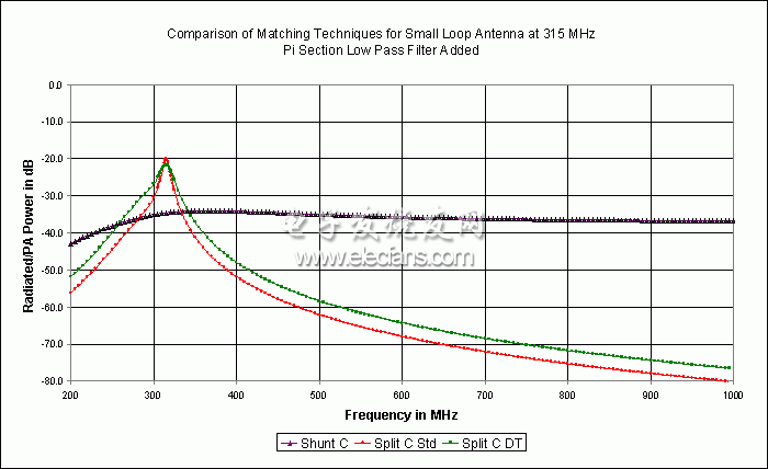
Figure 5. Power Transfer from a RFIC Transmitter to Loop Antenna. Lowpass Filter Added to Matching Section
Summary and Conclusions
For matching a small-loop antenna, it is important to remember that its equivalent series impedance is an inductance with a tiny series resistance, which consists predominantly of loss resistance and an even smaller radiation resistance. The small-loop antenna's equivalent parallel impedance is an inductance with a large parallel resistance (5k ohms to 50kohms). Either representation is difficult to match to a resistance of 100ohms to 300ohms.
The combination of a small capacitor in series with the loop and a larger capacitor in parallel with the series capacitor and loop, is a simple way to match the loop. An exact impedance match is very high-Q (ratio of loop reactance to resistance), which means that any drift in component value, frequency, or operating environment will degrade the match and raise the mismatch loss significantly. Choosing standard capacitor and inductor values that intentionally widen the match's bandwidth will produce a match more tolerant to component variations and the environment. The sacrifice for this wider bandwidth is more mismatch loss, but the loss is more predictable. Examples have been given for 315MHz and 433.92MHz.
When harmonic rejection is important, it is better to use two more components in the matching network to form a lowpass filter along with the matching network. The combination split-C and lowpass filter networks chosen in this application note can improve harmonic rejection by roughly 20dB over that of the simple split-C matching network.
The values in the matching networks presented here may need to be adjusted by the user slightly to accommodate stray reactances and losses in the circuit board or the matching components themselves. Care should also be taken to ensure that all the matching components are operating well below (two octaves preferred) their self-resonant frequencies (SRF).
What is more important than the specific value of each matching component, is the basic structure of these matching networks. The purpose of the split-C section is to transform the loop resistance value to a more reasonable range. The purpose of the pi-network lowpass filter is to reject higher frequencies, perform additional matching if needed, and establish the bandwidth of the match. As long as the user approaches the network with this in mind, the right component values can be found.
Notes
1 Balanis, C, Antenna Theory, Analysis, and Design, Harper and Row, NY, 1982
2 Stutzman, W.A., G.A. Thiele, Antenna Theory and Design, Wiley, NY, 1981
3 Dacus, F., Van Niekerk, J., and Bible, S., "Introducing Loop Antennas for Short-Range Radios", Microwaves & RF, July 2002, pp. 80-88.
 電子發(fā)燒友App










評(píng)論