Abstract: This application note describes how to transmit I2S audio data streams between two audio components across a single, shielded twisted-pair (STP) wire using the MAX9205 10-bit LVDS serializer and the MAX9206 10-bit LVDS deserializer.
Transmitting digital audio data using LVDS provides a robust, low-cost, high-bandwidth interface solution that can be easily added to existing hardware without impacting system resources. Digital audio data in the form of I2S streams, which are already available, can be transmitted to a different location in a vehicle with virtually no software overhead. By keeping the audio data in digital form, multiple ADCs, DACs, and wires can be eliminated from the system, thereby freeing up cost and board space for other features.
LVDS is already used to route video data from cameras, DVD players, and navigation systems to various displays in the vehicle. Its low signal amplitude and differential structure allow LVDS to transmit high-bandwidth data with low electromagnetic radiation.
Signals that leave a module in the wiring harness must be robust to withstand the harsh automotive environment and failure conditions. The LVDS bus needs to be AC-coupled to prevent damage if high-voltage short conditions occur. Since the MAX9205 does not automatically DC-balance the outgoing signal we must make sure that the data being transmitted is in fact DC-balanced. Since we are using no more than six of the ten available inputs we can use the remaining four inputs to DC-balance the transmitted data. The SCLK and WS signals are symmetrical signals so we only need to invert the random signals SDA0–3 and feed them into the unused inputs to ensure that the number of ones and zeros are equal for every 2-channel I2S packet transmitted.
To meet the setup and hold times for the MAX9205 and prevent excess jitter at the output of the MAX9206 deserializer, the I2S signals should be sampled when they are not changing state. Connect TCLK_R/F to GND to enable the MAX9205 to sample the inputs on the falling edge of the reference clock (TCLK). This assumes that the rising edge of TCLK corresponds to when SCLK changes state. If this is different than your configuration, make the appropriate adjustment to TCLK_R/F to ensure that the setup and hold times for the inputs are met. See Figure 1 below for the proper sampling of the I2S input signals.
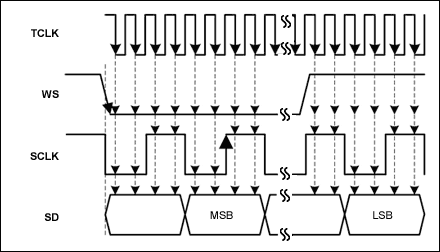
Figure 1. Sampling of I2S input signals.
Figure 2 illustrates the application schematic diagram.
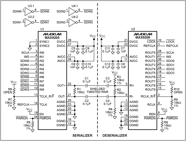
Figure 2. Schematic diagram for using the MAX9205/MAX9206 to transmit I2S audio data.
The left side of the schematic (labeled "Serializer") contains the circuit needed to serialize and transmit the LVDS audio data streams. Table 1 contains a list of components and signal descriptions for the serializer circuit.
Table 1. Component and Signal List for the Serializer Side
The right side of the schematic (labeled "Deserializer") contains the circuit needed to receive and deserialize the LVDS audio data streams. Table 2 contains a list of components and signal descriptions for the deserializer circuit.
Table 2. Component and Signal List for the Deserializer Side
1For an application note that details the advantages of LVDS for digital video transmission in automotive applications, refer to Application Note 4019: LVDS Offers Robust Video Interface for Automotive Applications.
Introduction
Low-voltage differential signaling—the most effective interface for in-vehicle digital video routing—can also be used as a low-cost solution to transmit digital audio data streams.1 This application note details how to use the MAX9205/MAX9206 10-bit LVDS serializer/deserializer (SerDes) ICs for transmitting up to four I2S audio data streams across STP wiring. Refer to the MAX9205/MAX9206 data sheets for detailed information on these ICs.The LVDS Serializer Advantage
Since each time an audio signal is converted between analog and digital domains the sound quality is degraded, it is important to keep audio data in digital form when possible in order to provide the best sound quality. The MOST? bus is designed for in-vehicle audio data transmission but is expensive to implement and overkill for most applications. For consumer audio equipment, S/PDIF is commonly used to transmit compressed audio data from one piece of audio equipment to another. However, S/PDIF does not have the bandwidth to transmit 5.1 or 7.1 digital audio in an uncompressed format and lacks a proven, robust physical layer for automotive applications.Transmitting digital audio data using LVDS provides a robust, low-cost, high-bandwidth interface solution that can be easily added to existing hardware without impacting system resources. Digital audio data in the form of I2S streams, which are already available, can be transmitted to a different location in a vehicle with virtually no software overhead. By keeping the audio data in digital form, multiple ADCs, DACs, and wires can be eliminated from the system, thereby freeing up cost and board space for other features.
LVDS is already used to route video data from cameras, DVD players, and navigation systems to various displays in the vehicle. Its low signal amplitude and differential structure allow LVDS to transmit high-bandwidth data with low electromagnetic radiation.
The MAX9205/MAX9206 Solution
The MAX9205 is designed to transmit 10-bit parallel data from a single reference clock. To transmit the I2S signals SCLK, WS, and SDA0–3 as data, we need a reference clock that is synchronous to SCLK and at least two times the frequency. The specified reference clock frequency range for the MAX9205 is between 16MHz and 40MHz. However, the IC will lock onto a reference clock as low as 10MHz. This allows us to use the commonly available clock frequency of 12.28MHz.Signals that leave a module in the wiring harness must be robust to withstand the harsh automotive environment and failure conditions. The LVDS bus needs to be AC-coupled to prevent damage if high-voltage short conditions occur. Since the MAX9205 does not automatically DC-balance the outgoing signal we must make sure that the data being transmitted is in fact DC-balanced. Since we are using no more than six of the ten available inputs we can use the remaining four inputs to DC-balance the transmitted data. The SCLK and WS signals are symmetrical signals so we only need to invert the random signals SDA0–3 and feed them into the unused inputs to ensure that the number of ones and zeros are equal for every 2-channel I2S packet transmitted.
To meet the setup and hold times for the MAX9205 and prevent excess jitter at the output of the MAX9206 deserializer, the I2S signals should be sampled when they are not changing state. Connect TCLK_R/F to GND to enable the MAX9205 to sample the inputs on the falling edge of the reference clock (TCLK). This assumes that the rising edge of TCLK corresponds to when SCLK changes state. If this is different than your configuration, make the appropriate adjustment to TCLK_R/F to ensure that the setup and hold times for the inputs are met. See Figure 1 below for the proper sampling of the I2S input signals.

Figure 1. Sampling of I2S input signals.
Figure 2 illustrates the application schematic diagram.

Figure 2. Schematic diagram for using the MAX9205/MAX9206 to transmit I2S audio data.
The left side of the schematic (labeled "Serializer") contains the circuit needed to serialize and transmit the LVDS audio data streams. Table 1 contains a list of components and signal descriptions for the serializer circuit.
Table 1. Component and Signal List for the Serializer Side
| DESIGNATION | QTY | DESCRIPTION |
| R1 | 1 | 100Ω ±1% Surface-mount resistor |
| R5, R7 | 2 | 10kΩ ±1% Surface-mount resistors |
| R8 | 1 | Unpopulated. Move R7 here to sample I2S signals on the rising edge of REFCLK. |
| C1, C2 | 2 | 0.1μF 25V ±5% Surface-mount ceramic capacitors |
| C5, C6 | 2 | 1nF 16V ±10% Surface-mount ceramic capacitors |
| C9, C10 | 2 | 0.1μF 25V ±10% Surface-mount ceramic capacitors |
| U1 | 1 | MAX9205EAI 10-Bit LVDS Serializer |
| U3, U4 | 2 | Dual inverter—ON Semi NL27WZ04DFT2G |
| SCLK | — | I2S serial clock |
| WS | — | I2S word select or left/right channel select |
| SDIN0–3 | — | I2S serial data stream |
| Active-low SDIN0–3 | — | Inverted I2S serial data stream input. This DC-balances the LVDS data stream to allow AC-coupling of the output. If AC-coupling is not necessary, then these signals can be tied to GND or used for control signals. |
| REFCLK | — | Reference clock. This reference clock must be at least two times the frequency and synchronous to SCLK. With a 48kHz I2S sample rate this clock must be at least four times SCLK. The inputs IN0–9 will be sampled on the falling edge of REFCLK with R8 populated and R7 unpopulated. |
| Active-low PWRDN | — | Power-down logic input. Pull down to put the part into shutdown mode. |
The right side of the schematic (labeled "Deserializer") contains the circuit needed to receive and deserialize the LVDS audio data streams. Table 2 contains a list of components and signal descriptions for the deserializer circuit.
Table 2. Component and Signal List for the Deserializer Side
| DESIGNATION | QTY | DESCRIPTION |
| R2 | 1 | 100Ω ±1% Surface-mount resistors |
| R3, R4, R6 | 2 | 10kΩ ±1% Surface-mount resistors |
| R9 | 1 | 10kΩ ±1% Surface-mount resistor. When populated ROUT_ is strobed out on the falling edge of REFCLK. |
| R10 | 1 | Unpopulated. Move R9 here to strobe ROUT_ out on the rising edge of REFCLK. |
| C3, C4 | 2 | 0.1μF 25V ±5% Surface-mount ceramic capacitors |
| C7, C8 | 2 | 1nF 16V ±10% Surface-mount ceramic capacitors |
| C11, C12 | 2 | 0.1μF 25V ±10% Surface-mount ceramic capacitors |
| U1 | 1 | MAX9205EAI 10-Bit LVDS Serializer |
| U2 | 1 | MAX9206EAI 10-Bit LVDS Deserializer |
| U3, U4 | 2 | Dual inverter—ON Semi NL27WZ04DFT2G |
| SCLK | — | I2S serial clock |
| WS | — | I2S word select or left/right channel select |
| SDO0–3 | — | I2S serial data stream |
| Active-low LOCK | — | Lock indicator. Active-low LOCK goes low when the PLL has achieved frequency and phase lock to the serial input, and when the framing bits have been identified. |
| REFCLK | — | Reference clock. This clock must be within ±500ppm of the MAX9205 reference clock frequency. |
| Active-low PWRDN | — | Power-down logic input. Pull down to put the part into shutdown mode. |
Conclusion
LVDS—the most effective interface for in-vehicle digital video routing—is also an effective interface for transmitting audio data. The MAX9205/MAX9206 LVDS serializer/deserializer ICs provide a simple, low-cost solution for transmitting multiple I2S audio streams between two points in a vehicle. Maxim’s next generation of LVDS products will continue to improve and support sending control and data across the same STP wire, thereby eliminating the need for an extra control interface.1For an application note that details the advantages of LVDS for digital video transmission in automotive applications, refer to Application Note 4019: LVDS Offers Robust Video Interface for Automotive Applications.
MOST is a registered trademark of MOST Corp.
 電子發(fā)燒友App





評論