Overview
All members of the High-Speed Microcontroller Family are designed to directly address up to 64kB of program and data memory. Occasionally, however, an application will require more memory than is either available on-chip or through the use of the 64kB memory map. The High-Speed Microcontroller Family includes many features which make it easy to address program and/or data memory greater than 64kB. Bit-addressable I/O ports allow single instruction modification of control lines, which can be used to bank switch or page between multiple memory devices. The ROMSIZE feature allows easy memory resizing for devices with on-chip memory.This application note discusses the expansion of both program and data memory. It is subdivided into three main categories: expanding program memory of ROMless devices beyond 64kB, using the ROMSIZE feature to expand on-chip program memory up to and beyond 64kB, and expanding data memory. It begins with an introduction to bank switching and software support techniques.
Bank Switching Theory
Expanded memory access beyond 64kB is most frequently done through bank switching. This technique uses one or more general purpose I/O lines as decode lines to address more memory. If a single large-capacity memory device is used, the additional signals can be used directly as address lines. If several smaller capacity memory devices are used, the signals can be used as chip selects. The basic unit of memory switched by the decode logic is called a bank or page. For example, if an I/O line was used to switch between two 64kB EPROMs, the memory would consist of two 64kB pages.Probably the biggest obstacle in using a paged memory scheme is the placement of the interrupt vector table. During most of the device operation, software can perform an orderly switch between pages. When an interrupt occurs, however, the device will immediately jump to the appropriate vector address, below 0070h. The software has no control over the bank configuration at this point, and the device will attempt to jump to the low end of the current bank to seek the vector table.
There are two approaches to solving this problem. The simplest is to duplicate the interrupt vector table at the low end of each page. In this way, the interrupt vector table will be available at all times, regardless of the current memory configuration. There are a number of disadvantages to this approach, however. It is an inefficient use of program memory as the interrupt vector table (approximately 120 bytes) and often the interrupt service routines, must be duplicated on every page. Also, some compilers do not directly support duplication of data across pages, complicating program generation. A more efficient approach is to reserve some lower portion of memory, which includes the interrupt vector table, so that it is not paged. This "common area" is directly accessible from any expanded bank without modification of the bank selection mechanism. Any time the processor performs a code fetch at this common area, hardware forces the memory to access this area, regardless of the current page. Careful design will allow the previous bank address to be saved, so that the device will return automatically when the operation in the common memory is complete. Interrupt service routine execution times can be reduced by locating them along with the interrupt vector table in the common area located at the low end of memory. Most of the examples in this application note designate the lower region of memory as the common area.
Software Support for Memory Expansion
For a paged memory scheme to work, it is necessary to fragment the code into pages and provide a means for the software to switch between pages. Care must be exercised when switching pages that the instruction flow will not be disturbed. There are two main approaches to this. The first is to switch pages "on the fly." This is demonstrated in the simple page expansion example which follows. This approach causes program execution to jump directly from one expanded page to another expanded page. One must exercise caution so that the bank switch will occur at a location that corresponds to the start of the next instruction in the next bank. Failure to correctly align the instructions may cause the next opcode fetch to occur in the middle of a multi-byte instruction, resulting in complete loss of program control.A better approach is to change banks from a location that will be unaffected by the change. This is most often a common or unpaged location in memory, such as a reserved location where the interrupt vector table is located. Any access to lower memory is automatically switched into the common memory by hardware. This eliminates the code alignment difficulties with the simple page expansion above, and the need to duplicate interrupt vectors and/or interrupt service routines on each memory page.
Many compilers and linkers directly support bank switching, and many of them include library functions for page switching. The documentation accompanying your compiler will provide information concerning its expanded memory support. Brief examples of assembly language support are listed after some of the examples below.
Care must be exercised if multiple pages are programmed into a single EPROM. Many EPROM programmers calculate program offsets using the address specified in the file, which can lead to misplaced code. For example, suppose that a paging scheme involves pages of code mapped into program space from 8000h to FFFFh. If the designer wished to locate a page at 10000h in the EPROM, he or she would normally select an offset of 10000h in the EPROM when loading the file into the programmer. All addresses in the hex file begin at 8000h, however, which the device programmer would add to 10000h. This would inadvertently place the page at 18000h, which was not the intended result. Various device programmers implement offsets in different ways, and the designer is advised to consult the documentation accompanying the device programmer for the best solution.
ROMless Program Expansion
The absence of on-chip program memory makes expanding the program memory of the DS80C320 relatively simple. Three approaches to expanding program memory are presented here. The first involves expansion of relatively small amounts of memory by duplicating vector tables and overlapping pages. The second example uses a common bank for interrupt vectors and interrupt service routines, and pages memory using several general purpose I/O lines. The last example uses a latched address to address large amounts of memory without using additional general purpose I/O lines.Simple Page Expansion
This example shows the simplest way of adding relatively small amounts of program memory. A single general purpose I/O line is used to provide up to 128kB of program memory. A single 27C010 128k byte EPROM is used, and is divided into two overlapping memory blocks. One general purpose I/O line, P1.0 in this case, is used to provide bank switch control. It is latched by a 74F74, which is clocked on the rising edge of the /PSEN\ signal. This synchronizes the bank switch with the memory cycle. This approach can be extrapolated to add even greater amounts of memory by using additional I/O lines. The hardware configuration for this example is shown in Figure 1.
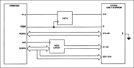
Figure 1. Simple page expansion example hardware.
The simplicity of the hardware comes at the cost of some software complexity, however. This example uses two banks, both of which contain the interrupt vector tables in the lower portion of memory. This is necessary because when the device is reset, P1.0 will be high, forcing the reset vector address to 10000h. Also, an interrupt may occur while executing code from either page, so the interrupt vectors must be available without software intervention. The interrupt vector table consumes approximately 115 bytes from locations 00000h to 00070h, and 10000h to 10070h. Additional space may be required if duplication of interrupt service routines is desired on each page.
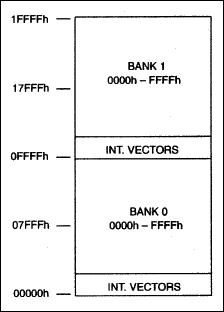
Figure 2. Simple page expansion example memory map.
This approach is most effective when page switching is kept to a minimum, i.e., executing straight runs of code. Code efficiency will be improved if the interrupt routines (not just the vectors) are small enough to be duplicated on each page as well. Data tables or strings accessed with MOVC instructions should be located on the same page as the instruction.
This approach directly modifies the page without modifying the program counter. This means that the starting location in the new page will be the same at the end of the bank switch routine in the new page. Consequently, instruction location between pages is critical. Figure 3 shows the timing relationship between a MOV P1, A instruction and the bank select signal. In this example, the MOV instruction is located at location 5A10h, and the first instruction on the new page is located at 5A14h.
The port pin which controls the bank selection will change during the first cycle following MOV instruction. The 74F74 latch causes the new bank selection to be valid on the prefetch during the execution of the second NOP. The first instruction on the new page must be at the address following the second NOP.
There are other ways of modifying port pins, and this scheme will work with 2 cycle instructions such as MOV direct, direct, and 1 cycle instructions such as SETB bit. There are only two requirements on the bank switching instructions. The first instruction on the new page must be at the address following the second NOP. Also, the instruction proceeding the MOV instruction must not be a MOVX. The MOVX instruction timing is variable because of stretch cycles, and could disturb the instruction flow.
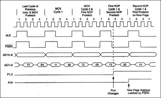
Figure 3. Bank switching timing diagram.
Common-Page Expansion Using I/O
The following two examples use a common-block approach in dealing with the problem of interrupt vector placement. This allows faster interrupt service times, and simplifies code construction. Both examples employ a paging scheme with 16 pages of 32kB each. Page 0, mapped at 0000h to 7FFFh, is the common area and contains the interrupt vector table and interrupt service routines. Address line A15 determines whether the common block, or one of the 15 expanded pages is addressed.
This example shows how to address up to 512kB of ROM using the general purpose I/0 lines on port 1 or 3 as bank switching controls. Bank 0 is a single 32kB page from 0 to 7FFFh. This common area will contain the interrupt vectors and commonly used subroutines. Expanded memory will be contained in 15 pages of 32kB mapped from 8000h to FFFFh. Bank control is provided by 4 general purpose I/O pins. The memory map is shown in Figure 4.
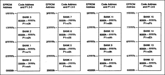
Figure 4. Common-page expansion memory example memory map.
The hardware configuration is shown in Figure 5. Bank control is provided by P1.0-3, decoded by 4 AND gates, requiring only a single IC package. When A15 is low, the device is forced to access only the lower 32kB of memory. This removes the need for software intervention when accessing the interrupt vector table in low memory. This example uses an 27C040 512KB EPROM.
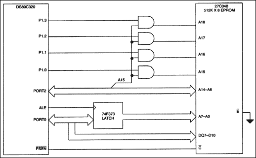
Figure 5. DS80C320 expanded memory example hardware configuration.
The following software example shows an assembly language routine to jump to a new location in any bank using I/O lines as shown in Figure 5. Before calling the bank switch subroutine, software pushes the new address and bank number onto the stack. It then calls a subroutine that pops the new bank address from the stack and places it on P1.0-3. The stack is then modified so that the subsequent RET instruction will return to the new program location. This is a simple demonstration of one of many possible ways to effect a bank-switch in assembly code.
Program Example: Jumping Between Banks Using I/O
;********************************************************************************
;Program BANKJMP1.ASM
;
;This program demonstrates one possible way to jump between banks in a common-
;page memory expansion configuration using I/O. Four general purpose I/O pins
;at P1.0-3 are used to control external bank selection.
;
;Software pushes the address in the new bank, as well as the new bank address
;onto the stack. The subroutine BANKJUMP, located at a non-paged address,
;modifies the page selection, and then repositions the stack pointer to the
;new address which was previously pushed onto the stack. The RET is then
;executed, resuming operation from the new address in the new page. Note that
;BANKJUMP can be called from any area in program memory.
;********************************************************************************
;Equate table
BANKMASK equ 0F0h ;P1.3-0 are used for bank selection.
NEWSUB_BANK equ 03h ;Subroutine NEWSUB is located on page 03h.

NEWSUB equ 0F000h ;Address of subroutine NEWSUB. If a
				;compiler is used, it may supply this
				;automatically.
;
cseg at 0 ;Reset vector.
	LJMP START
cseg at 100H ;Start of program
START: MOV P1, #0F0h ;Default to bank 0.
	MOV A, #low NEWSUB ;Low byte of NEWSUB address.
	PUSH A
	MOV A, #high NEWSUB ;High byte of NEWSUB address.
	PUSH A
	MOV A, #NEWSUB_BANK ;Bank address of NEWSUB.
	PUSH A
	LJMP BANKJUMP ;Call subroutine to switch operation
				;to new bank. This will transfer execution
				; to location NEWSUB in bank NEWSUB_BANK.
;********************************************************************************
;BANKJUMP - This subroutine pulls the new jump and page address off the stack.
; It modifies P1.0-3, and then modifies the stack pointer to point
; to the new address. It then Returns to the new jump location.
; This subroutine must be placed in a common, unpaged memory area.
;********************************************************************************
BANKJUMP: CLR EA ;Disable all interrupts.
	POP A ;Get the new page address off the stack
	ANL P1, #BANKMASK ;and modify only P1.0-3 to new bank
	ORL P1, A ;address.
	SETB EA ;Reenable interrupts.
	RET ;Stack pointer is now at new return
				;address. Program will begin executing
				;from new bank.
Common-Page Expansion Using Latched Data
One drawback to the above design is that it requires I/O lines as bank controls. Some I/O intensive applications may not be able to spare port pins for bank switching. The following example uses a Lattice Semiconductor GAL26V12 programmable logic device (PLD) to latch the bank select signals, rather than using dedicated I/O pins. This approach uses the same memory map as the previous example, with the exception that data memory from FFE0h to FFFFh is not accessible. These 32 bytes are inaccessible because A5 through A0 are not decoded, allowing a smaller, lower cost PLD to be used. Decoding more address lines would reduce the amount of inaccessible data memory, but would require a more complicated decoding mechanism.
The GAL26V12 performs the bank switching function based on a write to MOVX data memory. Any write to data memory from FFE0h to FFFFh is decoded, and the lower four bits of the data written to that address are used to configure the bank switch select lines. The hardware configuration is shown in Figure 6.
The source file for the PLD follows the illustration. It scans for any address in the selected range and latches the lower nibble of the data onto A15-A18 of the memory device. Addressing locations between 80000h will temporarily clear the bank select lines forcing the EPROM to read from bank 0 (0000h-7FFFh). As soon as the lower memory operation is complete, accesses to the upper half of memory (8000h-FFFFh) will automatically return to the previous bank because the bank address is still latched in the registered outputs of the PLD.
Although a variety of PLDs are suitable for this application, any device used must reset its outputs to 0 on power-up. This is necessary because upon power-up the device must be able to access the reset vector located at 0000h in bank 0. When selecting a PLD, the designer should be aware that many standard programmable logic devices are designed so that their outputs go high upon reset.
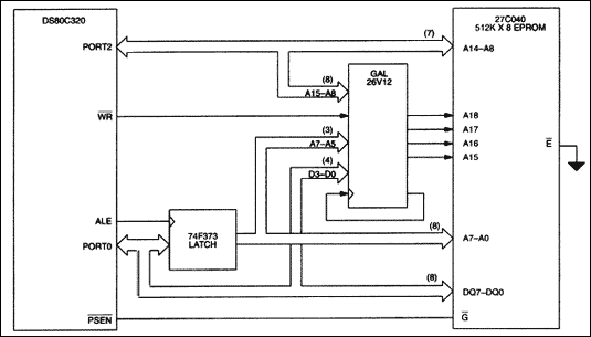
Figure 6. DS80C320 Latched address memory hardware example.
The following software example shows an assembly language routine to jump to a new location in any bank using latched data as shown in Figure 6. Before calling the bank switch subroutine, software pushes the new address and bank number onto the stack. It then calls a subroutine that pops the new bank address from the stack and writes it out to location FFFFh, where it is latched as the new bank address. The stack is then modified so that the subsequent RET instruction will return to the new program location.
Program Example: Jumping Between Banks Using Latched Addressing
;***************************************************************************
;Program BANKJMP2.ASM
;
;This program demonstrates one possible way to jump between banks in a common
;page memory expansion configuration using latched addressing.
;
;Software pushes the address in the new bank, as well as the new bank address
;onto the stack. The subroutine BANKJUMP, located at a non-paged address,
;modifies the page selection, and then repositions the stack pointer to the
;new address which was previously pushed onto the stack. The RET is then
;executed, resuming operation from the new address in the new page. Note that
;BANKJUMP can be called from any area in program memory.
;***************************************************************************
;Equate table
LATCH_ADR equ 0FFFFh ;Address of bank select latch.
NEWSUB_BANK equ 03h ;Subroutine NEWSUB is located on page 03h.
NEWSUB equ 0F000h ;Address of subroutine NEWSUB. If a compiler is
				; used, it may supply this automatically.
;
cseg at 0 ;Reset vector.
LJMP START

cseg at 100H ;Start of program

START: MOV A, #low NEWSUB ;Low byte of NEWSUB address.
	PUSH A
	MOV A, #high NEWSUB ;High byte of NEWSUB address.
	PUSH A
	MOV A, #NEWSUB_BANK ;Bank address of NEWSUB.
	PUSH A
	LJMP BANKJUMP ;Call subroutine to switch operation
				; to new bank.
;***************************************************************************
;BANKJUMP - This subroutine pulls the new jump and page address off the stack.
; It writes the new page address out to the PLD, where it is latched
; as the new page address. The RET then causes execution to the address
; specified in the function that called this routine. This subroutine
; must be placed in a common, unpaged memory area.
;***************************************************************************
BANKJUMP: CLR EA ;Disable all interrupts.
				; point to page address.
	POP A ;Get the new page address off the stack.
	MOV DPTR, #LATCH_ADR ;Write page address out to latch.
	MOVX @DPTR, A.
	SETB EA ;Restore interrupts.
	RET ;Stack pointer is now at new return
				; address. Program will begin executing
				; from new bank.
The source file for the GAL26V12 PLD is presented to aid the designer in developing his or her own devices. The file was written in the CUPL language, but can be easily be modified to work with other assemblers.
Program Example: GAL Program File
Name MEM_EXP;
Device g26v12;
/********************************************************************/
/** This CUPL file will program a GAL26V16 as a bank switching **/
/** latch to address up to 512kB of program memory. Any **/
/** MOVX write to addresses FFE0h through FFFFh will latch D0 - D3 **/
/** as the new bank selection. **/
/** **/
/** Any access to 0000h through 7FFFh in program memory will clear **/
/** the bank select lines for that operation only. This allows the **/
/** device to jump to interrupt vectors with no intervention, and **/
/** return to the same bank when finished. **/
/********************************************************************/
/*
/** PIN DEFINITIONS: These definitions are for 28 pin PLCC and DIP **/
/** Input pins **/
PIN 1 = CLKIN; Clock input for GAL latches.
PIN 2 = A15; Microcontroller address lines for address decode.
PIN 3 = A14;
PIN 4 = A13;
PIN 5 = A12;
PIN 6 = A11;
PIN 8 = A10;
PIN 9 = A9;
PIN 10 = A8;
PIN 11 = A7;
PIN 12 = A6;
PIN 13 = A5;
PIN 14 = D3; Microcontroller data lines to set bank selection.
PIN 15 = D2;
PIN 16 = D1;
PIN 17 = D0;
PIN 28 = WR_STROBE; Microcontroller write strobe
/** Output pins **/
PIN 20 = CLKOUT; Qualified microcontroller write strobe. It is fed
				; back into the GAL 26V12 CLK input. This
				; signal must be assigned to pin 20 or 22 because
				; it requires 12 product terms.
PIN 18 = A18_LATCH; Temporary latch of A18 memory signal.
PIN 19 = A17_LATCH; Temporary latch of A17 memory signal.
PIN 22 = A16_LATCH; Temporary latch of A16 memory signal.
PIN 23 = A15_LATCH; Temporary latch of A15 memory signal.
PIN 24 = MEMADR_18; Output to memory device pin A18.
PIN 25 = MEMADR_17; Output to memory device pin A17.
PIN 26 = MEMADR_16; Output to memory device pin A16.
PIN 27 = MEMADR_15; Output to memory device pin A15.
;PIN 7 = VCC
;PIN 21= GND

/** Qualify write strobe to detect valid bank latch write. **/
BANK_SEL = A15 & A14 & A13 & A12 & A11 & A10 & A9 & A8 & A7 & A6 & A5
CLKOUT = !WR_STROBE & BANK_SEL

/** BANK SELECT 0 GENERATION **/
A15_LATCH.D = D0
A15_LATCH.OEMUX = 0 ;Disable external expression of this signal.
MEMADR_15 = A15_LATCH.Q & A15

/** BANK SELECT 1 GENERATION **/
A16_LATCH.D = D1
A16_LATCH.OEMUX = 0 ;Disable external expression of this signal.
MEMADR_16 = A16_LATCH.Q & A15

/** BANK SELECT 2 GENERATION **/
A17_LATCH.D = D2
A17_LATCH.OEMUX = 0 ;Disable external expression of this signal.
MEMADR_17 = A17_LATCH.Q & A15

/** BANK SELECT 3 GENERATION **/
A18_LATCH.D = D3
A18_LATCH.OEMUX = 0 ;Disable external expression of this signal.
MEMADR_18 = A18_LATCH.Q & A15
Using the ROMSIZE Feature
The ROMSIZE feature allows software to dynamically reconfigure program memory size, permitting a portion of program memory to be switched between on- and off-chip. It provides an easy way to increase program memory to 64kB plus on-chip memory. In addition, it simplifies the task of building a bootloader for external programmable memory, such as FLASH, EEPROM, or Nonvolatile SRAM (NV SRAM).Using the ROMSIZE feature is very straightforward. Bits RMS2, RMS1, RMS0 (ROMSIZE.2-0) select the maximum amount of on-chip memory. The ROMSIZE select bits are Timed Access protected to ensure maximum software reliability. Any program memory accesses outside of the range defined by the ROMSIZE register will automatically be fetched externally via ports 0 and 2. External code fetches on devices with the ROMSIZE feature are performed in the same way as on all members of the High-Speed Microcontroller Family. The designer is reminded that if ports 0 and 2 will be used for external memory access, they should not be used as general purpose I/O ports.
The modification of the ROMSIZE register must be followed by a 2 machine cycle delay, such as executing 2 NOP instructions, before jumping to the new address range. Interrupts must be disabled during this operation, because a jump to the interrupt vector during the changing of the memory map can cause erratic results. The procedure to reconfigure the amount of on-chip memory is as follows:
- Jump to a location in program memory that will be unaffected by the change
- Disable interrupts by clearing the EA bit (IE.7)
- Write AAh to the Timed Access Register (TA;C7h)
- Write 55h to the Timed Access Register (TA;C7h)
- Modify the ROM Size Select bits (RMS2-0)
- Delay 2 machine cycles (2 NOP instructions)
- Enable interrupts by setting the EA bit (IE.7)
If the 0kB on-chip memory option is selected, extra precautions must be taken. It is necessary to duplicate the interrupt vector table in off-chip memory when switching the lower 1kB of program memory from on-chip to off-chip. In general, applications will find it most useful to reduce the on-chip memory no smaller than 1kB. This will maximize the addressable external memory range, while keeping the interrupt vectors on-chip. The 0kB option is most useful when the on-chip memory is only used as a boot loader.
Expanding Memory Beyond 64kB with the ROMSIZE Feature
Addressing more than 64kB of external memory in con-junction with the ROMSIZE feature is done similar to the ROMless method. The primary difference is that the ROMSIZE feature allows the designer to use the on-chip program memory as the "common" block. This simplifies the construction of external hardware, as the common block memory signal (the A15 signal in the examples presented) does not have to be decoded.The key to designing with the ROMSIZE feature is to incorporate the on-chip memory into the memory map with the most efficient memory utilization and simplest decoding method. There are many approaches to this problem, but only one will be presented here. This example uses 16kB of on-chip memory, plus eight 48kB pages of expanded memory located in a 27C040 512kB EPROM. This provides a total program memory of 400kB. The interrupt vectors and service routines are contained in the on-chip memory for fast access.
Figure 7 shows one possible memory map for use with the DS87C520 incorporating 16kB of on-chip EPROM. Note that program memory from 0000h to 3FFFh on each external page is not used. This greatly simplifies the design of the memory decode, requiring no external logic and one less I/O line. Figure 8 shows how to use three I/O lines to directly decode the upper address lines of the device. Software for this configuration is similar to that presented in previous examples.
It is also possible to use the ROMSIZE feature in conjunction with a latched bank address on the MOVX bus. Similar to the ROMless example, this approach does not require dedicated I/O pins for bank switching. Because the use of on-chip program memory allows for a simpler decode circuit, less expensive PLDs may be used.
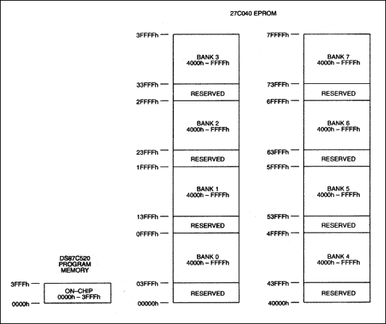
Figure 7. ROMSIZE Feature common-page expansion memory map.
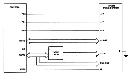
Figure 8. ROMSIZE Feature common-page I/O expansion.
Expanding the amount of data memory used by the microcontroller is the easiest form of memory expansion. Because there is no possibility of interfering with program execution, timing is not as critical. General purpose I/O lines can be connected directly to the address lines or chip enables of the memory device(s). The appropriate port pin can be directly modified to access the correct page prior to the memory operation. If the application requires all available I/O lines, then a latched bank address scheme demonstrated in the above examples can be used.
 電子發(fā)燒友App







評(píng)論