The 24Cxx series of 2-wire serial EEPROMs are widely used in 8051 microprocessor systems. Although the MAX7651/MAX7652 flash-programmable 12-bit data acquisition systems have 16K of internal flash memory, there are many "legacy" products that use small and inexpensive external memories.
This application note provides basic 2-wire WRITE and READ software subroutines. They can be easily modified to address additional features of EEPROMs, such as memory protection and bank addressing.
There are many derivatives of the 24C02 serial EEPROM, which include additional memory and page addressing. The 24C02 is widely used and is the part used in this example. Other derivative parts can use this code with minor modifications.
EEPROM Signals and Timing
The 24Cxx family uses two I/O lines for interfacing: SCL (Serial Clock) and SDA (Serial Data). SCL edges have different functions, depending on whether a device is being read from or written to. When clocking data into the device, the positive edges of the clock latch the data. The negative clock edges clock data out of the device.The SDA signal is bi-directional, and is physically an open-drain so that multiple EEPROMs or other devices can share the pin. Both SCL and SDA must be pulled high externally.
The protocol used by the EEPROM is based in part on an ACK (acknowledge) bit sent by the EEPROM, if the data sent to it has been received. All addresses and data are sent in 8-bit words. The EEPROM sends the ACK as a low bit period during the ninth clock cycle. The EEPROM looks for specific transitions on the SCL and SDA pins to qualify READ and WRITE.
Data on the SDA pin may change only during the time SCL is low. Data changes during SCL high periods indicate a START or STOP condition. A START condition is a high-to-low transition of SDA with SCL high. All data transfers must begin with a START condition.
A STOP condition is a low-to-high transition of SDA with SCL high. All data transfers must end with a STOP condition. After a READ, the STOP places the EEPROM in a standby power mode. Refer to Figure 1 for START and STOP conditions.
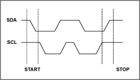
Figure 1. START and STOP conditions.
Device Addressing
The 24C02 has 3 physical pins, designated A2, A1, and A0, which are tied to logic 1 or 0 levels. This allows eight unique hardware addresses, so that up to eight 24C02s can share the SCL and SDA lines without conflict. There is an internal address comparator that looks for a match between the address sent by the master controller and the 24C02's unique 7-bit address, determined in part by A2, A1, and A0. Refer to Table 1below.Table 1. 24C02 Device Address
|
|
? | ? | ? | ? | ? | ? |
|
|
|
|
1 |
0 |
A2 |
A1 |
A0 |
|
The device address is sent immediately after a START condition. The first four bits are the sequence "1010", which is a simple "noise filter" which prevents a random noise burst on the lines from accessing the device. The last bit sent is a 1 for READ and a 0 for WRITE. The code example below is for random READ/WRITE operations. The part can also perform Page Write/Sequential Read with slight code modifications. See the 24C02 data sheet for more information.
Byte Write to Memory
The Byte Write sequence is shown in Figure 2. After receiving a START condition and a device address, the EEPROM sends an ACK if the device address matches its own unique address. The MAX7651 waits for the ACK and aborts communication if it is not present. Next, an 8-bit byte address is sent, followed by another ACK. The MAX7651 then sends the 8-bit data byte, waits for the third ACK, and sends a STOP condition.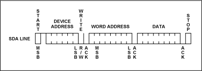
Figure 2. WRITE operation.
It is important to note that after the STOP condition is received, the EEPROM internally waits for the data to be stored into its internal memory array. This can take as long as 10ms. The 24C02 will ignore attempted accesses while the internal EEPROM is being programmed. The part can be polled for completion of the internal write cycle. This involves sending another START condition (also called a REPEATED START), followed by the device address byte. Note, in this case, there is no STOP condition sent. The EEPROM will send an ACK if the internal programming cycle is completed. The MAX7651 can also be programmed to wait 10ms before proceeding.
Byte Read from Memory
Reading a byte from the 24C02 EEPROM at a random address requires that a dummy WRITE operation be performed before the READ. See Figure 3.The sequence is:
- START condition
- Send device address with R/~W = 0 'dummy WRITE' command
- Wait for ACK
- Send byte memory address
- Wait for ACK
- Send REPEATED START condition
- Send device address with R/~W = 1 (READ command)
- Wait for ACK
- Read the 8 data bits into the MAX7651, MSB first
- No ACK
- STOP condition
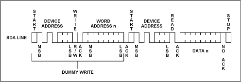
Figure 3. READ operation.
Code Example
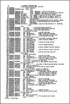
The following assembly language code example assumes a 24C02 EEPROM addressed at device 0H (i.e., A2 = A1 = A0 = ground). The MAX7651 uses two unused general-purpose I/O port pins to bit-bang the serial clock (SCL) and the bi-direction data line (SDA). Two internal RAM locations are needed: EE_ADDR stores the byte address and EE_DATA stores the data.; EEPROM ROUTINES FOR THE 24C02, with A2 = A1 = A0 = 0
| EE_WRITE: | CALL | EE_START | ; SEND A START FLAG TO THE EEPROM |
| MOV | A,#0A0H | ; SPECIFY A WRITE EEPROM @ ADDRESS 0H | |
| CALL | SHOUT | ; SHIFT OUT THE DEVICE ADDRESS | |
| JC | WR_ABORT | ; ABORT IF NO ACK FROM EEPROM | |
| MOV | A,EE_ADDR | ; GET EEPROM MEMORY ADDRESS | |
| CALL | SHOUT | ; SHIFT OUT THE MEMORY ADDRESS | |
| JC | WR_ABORT | ; ABORT IF NO ACK FROM EEPROM | |
| MOV | A, EE_DATA | ; GET THE DATA TO BE WRITTEN | |
| CALL | SHOUT | ; SHIFT OUT THE DATA | |
| JC | WR_ABORT | ; | |
| CLR | C | ; | |
| WR_ABORT: | CALL | EE_STOP | ; SEND STOP CONDITION TO EEPROM |
; WAIT FOR WRITE TIME OF THE 24C02 {10ms}
; THE EEPROM TAKES 10ms TO INTERNALLY STORE THE DATA. YOU CAN EITHER
; PUT THE MICROCONTROLLER IN A WAIT STATE, OR CONTINUE WITH EXECUTION,
; KEEPING IN MIND THAT THE EEPROM DATA IS NOT STORED FOR 10ms!
| RET | ; GO BACK TO MAIN PROGRAM |
; READ THE EEPROM DATA - FIRST PERFORM 'DUMMY WRITE'
| EE_READ: | MOV | EE_DATA,#00H | ; CLEAR OLD DATA |
| CALL | EE_START | ; SEND A START FLAG TO EEPROM | |
| MOV | A,#0A0H | ; SPECIFY A WRITE TO EEPROM @ ADDRESS 0H | |
| CALL | SHOUT | ; PERFORM 'DUMMY WRITE' | |
| JC | RD_ABORT | ; ABORT IF NO ACK | |
| MOV | A,EE_ADDR | ; LOAD EEPROM MEMORY LOCATION | |
| ? | ; FROM WHICH TO READ | ||
| CALL | SHOUT | ; WRITE EEPROM MEMORY LOCATION | |
| JC | RD_ABORT | ; ABORT IF NO ACK |
; NOW READ THE DATA!
| EE_WRITE: | CALL | EE_START | ; SEND A START FLAG |
| MOV | A,#0A1H | ; SPECIFY A READ FROM EEPROM | |
| CALL | SHOUT | ; SHIFT OUT EEPROM ADDRESS | |
| JC | RD_ABORT | ; ABORT IF NO ACK | |
| CALL | SHIN | ; SHIFT IN THE DATA FROM EEPROM | |
| MOV | EE_DATA,A | ; STORE THE DATA | |
| CALL | NAK | ; SEND A NAK (NO ACKNOWLEDGE) TO THE | |
| ; EEPROM | |||
| CLR | C | ; CLEAR ERROR FLAG | |
| RD_ABORT: | CALL | EE_STOP | ; ALL DONE |
| RET | ; |
; EE_START BIT-BANGS A START SEQUENCE TO EEPROM (HI-TO-LOW SDA TRANSITION
; WITH SCL HIGH).
| EE_START: | SETB | SDA | |
| SETB | SCL | ; SET BOTH BITS | |
| NOP | ; DELAY | ||
| CLR | SDA | ; START CONDITION; SDA HI TO LOW TRANSITION | |
| NOP | |||
| NOP | ; EEPROM ACCESS TIME DELAY | ||
| CLR | SCL | ||
| CLR | C | ; CLEAR ERROR FLAG | |
| RET | ; ALL DONE |
; EE_STOP SENDS A STOP SEQUENCE TO THE EEPROM (LOW-TO-HIGH SDA TRANSITION
; WITH SCL HIGH).
| EE_STOP: | CLR | SDA | ? |
| NOP | |||
| NOP | |||
| SETB | SCL | ||
| NOP | |||
| NOP | ; SETUP TIME DELAY | ||
| SETB | SDA | ; SEND A STOP CONDITION | |
| RET |
; SHOUT SHIFTS DATA OUT TO THE EEPROM
| SHOUT: | PUSH | B | |
| ? | MOV | B,#8 | ; SAVE B AND LOAD BIT COUNT |
| EEOUT: | RLC | A | ; SHIFT BIT LEFT (RLC=ROTATE LEFT THROUGH |
| ; CARRY) | |||
| MOV | SDA,C | ; GET DATA BIT FROM CARRY | |
| NOP | |||
| SETB | SCL | ; CLOCK IN 1-BIT | |
| NOP | ; CLOCK HIGH TIME | ||
| ? | CLR | SCL | ; CLOCK IS NOW LOW |
| DJNZ | B,EEOUT | ; DO IT 8 TIMES | |
| SETB | SDA | ; RELEASE SDA FOR ACK | |
| NOP | |||
| NOP | |||
| SETB | SCL | ; ACK CLOCK | |
| NOP | |||
| MOV | C,SDA | ; GET THE ACK | |
| CLR | SCL | ; CLEAR THE CLOCK BIT | |
| POP | B | ; RESTORE WHATEVER B WAS | |
| RET |
; SHIN SHIFT DATA IN FROM THE EEPROM
| SHIN: | SETB | SDA | ; MAKE SDA AN INPUT |
| PUSH | B | ||
| MOV | B,#8 | ; SAVE B AND SET BIT COUNTER | |
| EEIN: | NOP | ||
| SETB | SCL | ; SET CLOCK | |
| NOP | |||
| NOP | ; EEPROM ACCESS TIME | ||
| SETB | SDA | ; SET = 1 SO USED AS INPUT | |
| MOV | C,SDA | ; READ 1-BIT | |
| RLC | A | ; SHIFT BIT LEFT | |
| CLR | SCL | ; CLEAR CLOCK BIT | |
| DJNZ | B,EEIN | ; GET NEXT BIT IF LESS THAN 8 BITS READ | |
| POP | B | ||
| RET |
; ACK SENDS AN EEPROM ACKNOWLDEGE
| ACK: | CLR | SDA | |
| NOP | |||
| NOP | |||
| SETB | SCL | ; CLOCK THE ACK | |
| NOP | |||
| CLR | SCL | ; BRING CLOCK LOW | |
| RET |
; NAK SENDS A NO ACKNOWLEDGE
| NAK: | SETB | SDA | |
| NOP | |||
| NOP | |||
| SETB | SCL | ; CLOCK THE NAK | |
| NOP | |||
| CLR | SCL | ; BRING CLOCK LOW | |
| RET |
$EJECT
 電子發(fā)燒友App









評論