Introduction
The TMS320C54x family of devices is fixed-point digital signal processors (DSP) offered by Texas Instruments. This family, referred to as '54x, implements several types of serial port operations. The buffered serial port, commonly referred to as the BSP, provide full-duplex communication capabilities with either a T1 or an E1 data structure, due to these ports supporting the use of frame synchronization strobes. The BSP allows transfers of 8-, 10-, 12-, or 16-bit data packets. In the continuous mode, the frame synchronization pulse occurs when the data transmission (or reception) is initiated. Any further pulses applied to this input during the reception or transmission of data packets will cause a receive or transmit abort condition, and one packet of data will be lost. In the burst mode, a frame synchronization pulse occurs for every packet. To ensure that each time slot of the T1 or E1 data stream is properly transferred between the '54x and the DS21x5y single-chip transceiver (SCT), this application note outlines how to interconnect these two IC’s for operation in both the continuous and burst modes.TMS320C54x BSP Continuous Mode Operation
The continuous mode of operation in the '54x is selected by setting FSM = 0 in the Serial Port Control (SPC) register. The use of the Autobuffering Unit (ABU) is outlined here, as this will allow at least 125μs between Buffer- Full/Buffer Empty interrupts to the CPU. The minimal buffer size for either transmit or receive path would be 48 bytes, since there are 24 8-bit time slots per T1 frame (32 for E1). Please refer to Section 9.1 Introduction to the Serial Ports, of the TMS320C54x Reference Set, Volume 1: CPU and Peripherals for complete initialization and descriptions of BSP and ABU operations.
Figure 1. Continuous Mode Transmit Timing (External Frame).
Note that in Figure 1, the Transmit synchronization pulse occurs at the location where the DS21x5y inserts a frame bit. Since the DS21x5y will internally generate the frame bit, and the '54x is not using the bit position where a frame synchronization pulse occurs, this allows a glueless interface between these two devices on this signal.

Figure 2. Continuous Mode Receive Timing (External Frame).
Note that in Figure 2, the Receive synchronization pulse occurs at the location where the DS21x5y located a frame bit in the receive stream. Since the '54x sees this as a FSR pulse reception during a Receive in Progress condition, the current receive buffer load will be aborted, and start over with the next received bit. This is acceptable, since the FSR did not occur during a valid bit condition (occurring during the framing bit, or Fbit position. The TMS320C54x will start clocking into the RSR with the first bit of the time slot following the Fbit. This allows a glueless interface between these two devices on this signal.
TMS320C54x BSP Continuous Mode and the DS21x5y Signal Descriptions
The table below describes how the TMS320C54x BSP connects to the DS21x5y when operating the TMS320C54x in the continuous mode. A short description of each signal is given. (Note: all descriptions for the TMS320C54x device are taken from the data sheet entitled, TMS320C54x,TMS320LC54x, TMS320VC54x Fixed-Point Digital Signal Processors.)Table 1.
| TMS320C54x BSP SIGNAL | DS21x5y SIGNAL |
| BCLKR (Buffered Receive Clock). Input only. External clock signal for clocking data from the Buffered Data-Receive (BDR) pin into the buffered serial port receive shift registers (RSRs). | RCLK (Receive Clock). Output only. Either a 1.544MHz (DS21x52), or a 2.048 MHz (DS21x54) clock that is used to clock data through the receive-side framer. (Note: to ensure that this clock is recovered from the LIU's receive data path, the RCLKO pin should be tied to the RCLKI pin.) |
| BDR (Buffered Data Receive). Input only. Buffered serial receive data, clocked directly into the serial port receive shift registers (RSRs). | RSER (Receive Serial Data). Output only. Received NRZ data. Updated on the rising edges of RCLK when the receiveside elastic store is disabled. Updated on the rising edge of RSYSCLK when the elastic store is enabled. |
| BFSR (Buffered Frame Synchronization Receive). Input only. Frame synchronization pulse for the receive input. The falling edge of the BFSR pulse initiates the data-receive process, beginning the clocking of data into the RSR. | RSYNC (Receive Sync). Configured for an output. An extracted pulse one RCLK wide, is output when an entire T1 (DS21x52) or an entire E1 (DS21x54) frame is beginning. |
| BCLKX (Buffered Transmit Clock). Configured for an input1. Clock signal for clocking data from the serial port transmit shift register (XSR) to the Buffered Data Transmit (BDX) pin. BCLKX is configured as an input by clearing the MCM bit in the serial port control register (SPCR). | TCLK (Transmit Clock). Input only1. Either a 1.544 MHz (DS21x52), or a 2.048 MHz (DS21x54) clock that is used to clock data through the transmit-side framer. (Note: to ensure that this clock is recovered from the LIU's receive data path, the LIUC pin should be tied high.) |
| BDX (Buffered Data Transmit). Configured for an output. Buffered serial-port-transmit output. Serial data is transmitted from the serial port transmit shift register (XSR) through this pin. The EMU1/OFF signal should be set to 1, therefore preventing the BDX pin from going into a high-impedance state when not transmitting. | TSER (Transmit Serial Data). Input only. Transmit NRZ serial data. Sampled on the falling edge of TCLK when the transmit-side elastic store is disabled. Sampled on the falling edge of TSYSCLK when the transmit-side elastic store is enabled. |
| BFSX (Buffered Frame Synchronization Transmit). Configured for an input2. Frame synchronization pulse for the transmit output. The falling edge initiates the data-transmit process, beginning the clocking of the XSR. Following reset, the BFSX pin's default operating condition is that of an input. | TSYNC (Transmit Sync). Configured for an output2. A single TCLK wide pulse on this pin will establish a frame boundary on the transmit side. |
2Normally the device attached to the DS21x5y will supply the TSYNC signal. But in this case the TMS320C54x family will operate in the continuous mode, and therefore would not output frame synchronization signals compatible with either a T1 or an E1 frame boundary. Therefore, the DS21x5y should be the source of this signal.
TMS320C54x BSP Burst Mode Operation using T1 Frames
The burst mode of operation in the '54x is selected by setting FSM = 1 in the Serial Port Control (SPC) register. Like in the continuous mode of operation, the use of the Autobuffering Unit (ABU) allows at least 125μs between Buffer-Full/Buffer Empty interrupts to the CPU. The minimal buffer size for either transmit or receive path would be 48 bytes, since there are 24 8-bit time slots per T1 frame (32 for E1). Please refer to Section 9.1 Introduction to the Serial Ports, of the TMS320C54x Reference Set, Volume 1: CPU and Peripherals for complete initialization and descriptions of BSP and ABU operations.
Figure 3. Burst Mode Transmit Timing (External Frame).
Note that in Figure 3, the transmit synchronization pulse BFSX occurs at the LSB of each time slot of the DS21x52 transmit datastream. The requirements needed for this signal is very much like the TCHCLK signal of the DS21x5y, with the exception of the 24th time slot. This exception will cause some external logic requirements to be implemented (see below).

Figure 4. Burst Mode Receive Timing (External Frame).
Note that in Figure 4, the receive synchronization pulse BFSR occurs at the LSB of each time slot of the DS21x52 transmit datastream. The requirements needed for this signal is very much like the RCHCLK signal of the DS21x5y, with the exception of the 24th time slot. Like the transmit side, this exception will cause some external logic requirements to be implemented to ensure proper operation.
External Logic Requirements for Burst Mode Using T1 Frames
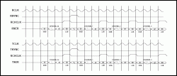
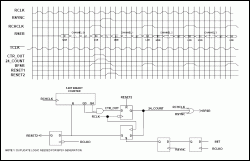
Using the TMS320C54x BSP's with the DS21x52 is not glueless, specifically if the user clocks data out of the SCT at a T1 frame rate. This is due to the insertion of the framing bit between the 24th time slot of the previous T1 frame and the first time slot of the current T1 frame. If the TCHCLK or the RCHCLK signal is directly interconnected into the BFSX or the BFSR signals, then the first T1 frame of the current frame will contain errors. Specifically, the first time slot's LSB will be the framing bit, and the MSB will be B7 of the time slot.Figure 5 outlines the timing strobes available on the DS21x52 when clocking data out at T1 data rates. These signals will be used to generate the proper timing signals outlined in Figure 6. Figure 6 outlines the proper burst mode timing requirements needed to ensure proper operation of the TMS320C54x with the DS21x52 using T1 timing, along with the external logic needed to implement the proper timing requirements.
More Detailed Image.
Figure 5. Timing Strobes Available on the DS21x52–T1 Timing.
More Detailed Image.
Figure 6. Generating BFSR1 for Proper Burst Mode Operation of the TMS320C54x–T1 Clocking.
TMS320C54x BSP Burst Mode Operation Using a 2.048MHz Systems Clock
Another option which uses less external logic interfacing from the TMS320C54x to the DS21x5y in burst mode would be using a 2.048MHz clock into the TSYSCLK and RSYSCLK inputs of the SCT, and enabling the elastic stores. The SCT will then do a rate conversion between the T1 line rate and the 2.048MHz system clock. This is accomplished internal to the SCT by forcing time slots 0, 4, 8, 12, 16, 20, 24, and 28 to all ones on the receive side, or ignoring these same time slots on the transmit path. The F-bit will be deleted (unless selected to pass through in the LSB of time slot 0).In the case where the elastic store's system clock is locked to its network clock, the elastic store's minimum delay mode can be used. RSYNC would then be configured as an output and then connected to TSSYNC. Since both the transmit and the receive path are frequency-locked, then RSYSCLK and TSYSCLK can be connected together.
Also, with a 2.048MHz system clock, the TCHCLK signal of the DS21x5y will be connected directly to the BFSX signal of the TMS320C54x. Likewise, the RCHCLK signal of the DS21x5y will be connected directly to the BFSR signal of the TMS320C54x. Very minimal external logic would then be required to synchronize these signals to the RSYNC and TSSYNC signals during initialization.
Figure 7 shows the block diagram of how the TMS320C54x and the DS21x5y can be connected when operating with the elastic stores enabled and configured for the minimal delay mode and using a 2.048MHz systems clock.
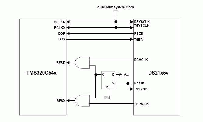
Figure 7. Block Diagram of the TMS320C54x and the DS21x5y Using a 2.048MHz System Clock Locked to the Network Clock.
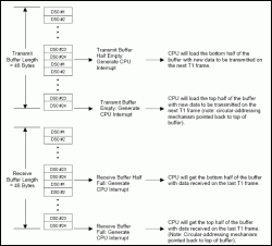
Autobuffering Unit (ABU) T1/E1 Operation The ABU will implement CPU interrupts when its transmit and receive buffers are halfway or entirely filled or emptied. By checking either the RH bit or the XH bit in the BSP Control Extension (BSPCE) Register, the CPU can operate on the data in the opposite half of the buffer being operated on. The circular addressing mechanism will automatically update the buffer pointers to ensure that once the end of the buffer is reached, the next reception will occur at the beginning of the buffer.
Consider the case where the input into the BSP is a T1 datastream. Initialization of the circular addressing mechanism would begin by loading both BKX/R with the exact size of the desired buffer (each buffer in this case being two T1 frames, or 48 bytes). Completion of the initialization would end with the base address values of these two 48-byte buffers within the 2k word block dedicated to this operation along with the initial starting address within the buffer (normally 00H). Loading would be into the ARX/R registers. Upon starting the ABU, an interrupt will occur when either of the buffers are half full (or empty). At this point the CPU should see which buffer caused the interrupt, and then see if the interrupt was caused by a half-full (empty) or full (empty) buffer. The CPU would then service the data in the portion of the buffer which is opposite of the buffer currently being serviced by the ABU. This allows the CPU to be working on the previous T1 frame of data. Figure 8 outlines this entire procedure when using a T1 datastream.
When interfacing to an E1 datastream, the buffer sizes will now be 64 bytes, since an E1 frame consists of 32 time slots, each with a single byte of data.
More Detailed Image.
Figure 8. Autobuffering Unit Operation.
DS21x5y Information
If you have further questions on interfacing with the DS2x5y family of SCTs, please contact the Telecommunication Applications support team via email telecom.support@dalsemi.com or call 972-371-6555.For more information about the DS21x5y, please consult the DS21x5y data sheets available on our website. References:
- TMS320C54x,TMS320LC54x,TMS320VC54x Fixed-Point Digital Signal Processors, Literature number SPRS039B - February 1996 - Revised February 1998, Texas Instruments, Inc.
- TMS320C54x DSP Reference Set - Volume 1: CPU and Peripherals, Literature number SPRU131F - April 1999, Texas Instruments, Inc.
 電子發(fā)燒友App










評(píng)論