Abstract: A SOT step-down DC-DC converter efficiently "steals" power from a parallel port while a SIM/Smart Card level shift integrated circuit (IC) completes the interface. This allows the parallel port to power, and communicate with, low voltage logic. The same techniques can also be applied to USB designs.
For portable-sensing and data-acquisition applications, a laptop computer and its parallel port (LPT) make good bedfellows. Yet in the effort to extend battery life, many microprocessors and entire systems operate with logic levels down to 1.8V. The LPT port's 5V output signals don't easily support the low-voltage logic required to increase battery life and achieve longer data-acquisition times.
Because dynamic power consumption for a microprocessor or clocked circuit is predominately a function of voltage (P = CV2f), logic systems that operate off the parallel port at below 5V can substantially conserve power. The circuit shown in the figure accepts data from the LPT port and delivers up to 100mA at 2V. Efficiency is as high as 94%. Translating 5V logic levels at the LPT-port data pins down to 2V, the circuit also offers ESD protection.
The low-voltage surface-mount IC labeled U1—a step-down DC-DC converter with built-in MOSFETs and a synchronous rectifier—forms a simple and highly efficient 2V source. Feedback resistors R1 and R2 set the output voltage as low as 1.25 V. (Voltage is set at 2V in the example circuit.) U1's shutdown pin connects directly to bit D1 of the 5V LPT control port (pin 14), letting the device be enabled and disabled with software.
When enabled, U1's soft-start capability limits the inrush current. Schottky diodes D1 through D3 act in conjunction with pins 5 through 9 of the 5V LPT data port to provide power for the converter. Software also easily enables and disables the data-port pins.
As a low-voltage SIM/Smart-Card level translator, U2 translates the logic levels from 5 to 2V. U2 also provides ESD protection to the inputs. The input side of the low-voltage translator operates at 5V logic levels and is powered by input capacitor C1 at approximately 5V. U2's output side is powered by the 2V supply. Data is read into the LPT status port (pin 12) serially; clock (CLK) and chip-select (active-low CS) signals are derived from the LPT data port and software.
The example data interface consists of an 8-bit parallel-load shift register (U3) and an open-drain logic gate (U4). It reads U2's I/O pin and supplies parallel data. Software in the PC toggles the CLK and active-low CS lines to load and shift this parallel data into the program. The C++ software and text is configured to convert parallel data from the shift register to a serial format. After minor modifications, however, it can be configured to support a microcontroller interface or a serial SPI, I2C, or SMBus interface.
Therefore, this circuit can send data to an SPI, I2C, or SMBus serial interface, or to an 8-bit parallel-out serial shift register such as the SN74HC164, which can operate at 2V. Many devices available today take advantage of these power savings by operating down to 1.5V.
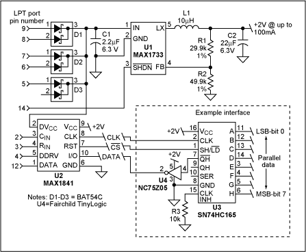
Figure 1. To save power, this circuit converts the 5V LPT parallel interface of a laptop computer to a parallel interface operating at a lower voltage.
A similar version of this article appeared in the June 24, 2002 issue of Electronic Design magazine.
For portable-sensing and data-acquisition applications, a laptop computer and its parallel port (LPT) make good bedfellows. Yet in the effort to extend battery life, many microprocessors and entire systems operate with logic levels down to 1.8V. The LPT port's 5V output signals don't easily support the low-voltage logic required to increase battery life and achieve longer data-acquisition times.
Because dynamic power consumption for a microprocessor or clocked circuit is predominately a function of voltage (P = CV2f), logic systems that operate off the parallel port at below 5V can substantially conserve power. The circuit shown in the figure accepts data from the LPT port and delivers up to 100mA at 2V. Efficiency is as high as 94%. Translating 5V logic levels at the LPT-port data pins down to 2V, the circuit also offers ESD protection.
The low-voltage surface-mount IC labeled U1—a step-down DC-DC converter with built-in MOSFETs and a synchronous rectifier—forms a simple and highly efficient 2V source. Feedback resistors R1 and R2 set the output voltage as low as 1.25 V. (Voltage is set at 2V in the example circuit.) U1's shutdown pin connects directly to bit D1 of the 5V LPT control port (pin 14), letting the device be enabled and disabled with software.
When enabled, U1's soft-start capability limits the inrush current. Schottky diodes D1 through D3 act in conjunction with pins 5 through 9 of the 5V LPT data port to provide power for the converter. Software also easily enables and disables the data-port pins.
As a low-voltage SIM/Smart-Card level translator, U2 translates the logic levels from 5 to 2V. U2 also provides ESD protection to the inputs. The input side of the low-voltage translator operates at 5V logic levels and is powered by input capacitor C1 at approximately 5V. U2's output side is powered by the 2V supply. Data is read into the LPT status port (pin 12) serially; clock (CLK) and chip-select (active-low CS) signals are derived from the LPT data port and software.
The example data interface consists of an 8-bit parallel-load shift register (U3) and an open-drain logic gate (U4). It reads U2's I/O pin and supplies parallel data. Software in the PC toggles the CLK and active-low CS lines to load and shift this parallel data into the program. The C++ software and text is configured to convert parallel data from the shift register to a serial format. After minor modifications, however, it can be configured to support a microcontroller interface or a serial SPI, I2C, or SMBus interface.
Therefore, this circuit can send data to an SPI, I2C, or SMBus serial interface, or to an 8-bit parallel-out serial shift register such as the SN74HC164, which can operate at 2V. Many devices available today take advantage of these power savings by operating down to 1.5V.

Figure 1. To save power, this circuit converts the 5V LPT parallel interface of a laptop computer to a parallel interface operating at a lower voltage.
A similar version of this article appeared in the June 24, 2002 issue of Electronic Design magazine.
 電子發(fā)燒友App







評論