DS1875 Quick Reference Guide
Abstract: The DS1875 burst-mode PON controller with integrated monitoring allows programming to configure the alarms, warnings, lookup tables, and other functions. The programming necessitates a large register memory map. This application note provides a simplified view of the register map, which is convenient when programming the device.
Memory Map of the DS1875
The DS1875 burst-mode PON controller features 10 separate memory tables that are internally organized into 8-byte rows.The Lower Memory is addressed from 00h to 7Fh. It contains alarm and warning thresholds, flags, masks, several control registers, password entry area (PWE), and the Table Select byte.
Table 00h contains conversion results for MON5 through MON8.
Table 01h primarily contains user EEPROM (with PW1 level access), as well as some alarm and warning status bytes.
Table 02h is a multifunction space that contains configuration registers, scaling and offset values, passwords, interrupt registers, and other miscellaneous control bytes.
Table 03h is strictly user EEPROM that is protected by a PW2-level password.
Table 04h contains a temperature-indexed LUT for controlling the modulation voltage. The modulation LUT can be programmed in 2°C increments over the -40°C to +102°C range. Access to this register is protected by a PW2-level password.
Table 05h contains a temperature-indexed LUT. It allows the APC set point to change as a function of temperature to compensate for TE (tracking error). The APC LUT has 36 entries that determine the APC setting in 4°C windows between -40°C to +100°C. Access to this register is protected by a PW2-level password.
Table 06h contains a MON4-indexed LUT for controlling the M4DAC voltage. The MON4 LUT has 32 entries that are configurable to act as one 32-entry LUT of two 16-byte LUTs. When configured as one 32-byte LUT, each entry corresponds to an increment of 1/32 of the full scale. When configured as two 16-byte LUTs, the first 16 bytes and the last 16 bytes each correspond to 1/16 of full scale. Either of the two sections is selected with a separate configuration bit. Access to this register is protected by a PW2-level password.
Table 07h contains a temperature-indexed LUT for controlling the PWM reference voltage (integration of FB input). The PWM LUT has 36 entries that determine the APC setting in 4°C windows between -40°C to +100°C. Access to this register is protected by a PW2-level password.
Table 08h contains a temperature-indexed LUT for controlling the BIAS current. The BIAS LUT can be programmed in 2°C increments over the -40°C to +102°C range. Access to this register is protected by a PW2-level password.
Auxiliary memory (Device A0h) contains 256 bytes of EE memory accessible from address 00h – FFh. It is selected with the device address of A0h.
DS1875 Memory Map
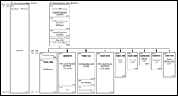
More detailed image (PDF, 8kB)
Figure 1. DS1845 memory map.
Register Reference
The following tables provide an easy reference to the Lower Memory and Tables 00h, 01h, and 02h. For a description of the functionality for each bit, please refer to the corresponding register in the data sheet. Tables 03h through 08h are LUTs that do not require a separate reference and, therefore, not included here. Please refer to the data sheet for detailed information about these tables.Note: RSVD is used as an acronym for Reserved.
Lower Memory
| Register Name | Register Addr | Bit7 | Bit6 | Bit5 | Bit4 | Bit3 | Bit2 | Bit1 | Bit0 |
| TEMP ALARM HI | 00h, 04h | S | 26 | 25 | 24 | 23 | 22 | 21 | 20 |
| TEMP WARN HI | 01h, 05h | 2-1 | 2-2 | 2-3 | 2-4 | 2-5 | 2-6 | 2-7 | 2-8 |
| TEMP ALARM LO | 02h, 06h | S | 26 | 25 | 24 | 23 | 22 | 21 | 20 |
| TEMP WARN LO | 03h, 07h | 2-1 | 2-2 | 2-3 | 2-4 | 2-5 | 2-6 | 2-7 | 2-8 |
| VCC ALARM HI | 08, 0C, 10,14, 18, 1C, 20, 24,28, 2Ch | 215 | 214 | 213 | 212 | 211 | 210 | 29 | 28 |
| VCC WARN HI | |||||||||
| MON1-4 ALARM HI | 09, 0D, 11, 15, 19, 1D, 21, 25, 29, 2Dh | 27 | 26 | 25 | 24 | 23 | 22 | 21 | 20 |
| MON1-4 WARN HI | |||||||||
| VCC ALARM LO | 0A, 0E, 12, 16, 1A, 1E, 22, 26, 2A, 2Eh | 215 | 214 | 213 | 212 | 211 | 210 | 29 | 28 |
| VCC WARN LO | |||||||||
| MON1-4 ALARM LO | 0B, 0F, 13, 17, 1B, 1F, 23, 27, 2B, 2Fh | 27 | 26 | 25 | 24 | 23 | 22 | 21 | 20 |
| MON1-4 WARN LO | |||||||||
| PW2 EE | 30h-5Fh | EE | EE | EE | EE | EE | EE | EE | EE |
| TEMP VALUE | 60h | S | 26 | 25 | 24 | 23 | 22 | 21 | 20 |
| 61h | 2-1 | 2-2 | 2-3 | 2-4 | 2-5 | 2-6 | 2-7 | 2-8 | |
| VCC VALUE | 62, 64, 66, 68, 6Ah | 215 | 214 | 213 | 212 | 211 | 210 | 29 | 28 |
| MON1-4 VALUE | 63, 65, 67, 69, 6Bh | 27 | 26 | 25 | 24 | 23 | 22 | 21 | 20 |
| RESERVED | 6C, 6Dh | 0 | 0 | 0 | 0 | 0 | 0 | 0 | 0 |
| STATUS | 6Eh | FETG STATUS | SOFT FETG | RSVD | TXF RESET | SOFT TXD | TXF STATUS | LOS STATUS | RDYB |
| UPDATE | 6Fh | TEMP RDY | VCC RDY | MON1 RDY | MON2 RDY | MON3 RDY | MON4 RDY | MON5/7 RDY | MON6/8 RDY |
| ALARM3 | 70h | TEMP HI | TEMP LO | VCC HI | VCC LO | MON1 HI | MON1 LO | MON2 HI | MON2 LO |
| ALARM2 | 71h | MON3 HI | MON3 LO | MON4 HI | MON4 LO | RSVD | RSVD | RSVD | RSVD |
| ALARM1 | 72h | RSVD | RSVD | RSVD | RSVD | BIAS HI | RSVD | TXP HI | TXP LO |
| ALARM0 | 73h | M3QT HI | RSVD | RSVD | RSVD | BIAS MAX | RSVD | RSVD | RSVD |
| WARN3 | 74h | TEMP HI | TEMP LO | VCC HI | VCC LO | MON1 HI | MON1 LO | MON2 HI | MON2 LO |
| WARN2 | 75h | MON3 HI | MON3 LO | MON4 HI | MON4 LO | RSVD | RSVD | RSVD | RSVD |
| RESERVED | 76h, 77h | RSVD | RSVD | RSVD | RSVD | RSVD | RSVD | RSVD | RSVD |
| DOUT | 78h | M3QT RESET | SOFT M3QT | RSVD | RSVD | D3 OUT | D2 OUT | D1 OUT | D0 OUT |
| DIN | 79h | INV M3QT | MUX M3QT | INV LOS | MUX LOS | D3 IN | D2 IN | D1 IN | D0 IN |
| RESERVED | 7Ah | RSVD | RSVD | RSVD | RSVD | RSVD | RSVD | RSVD | RSVD |
| PASSWORD ENTRY | 7Bh | 231 | 230 | 229 | 228 | 227 | 226 | 225 | 224 |
| 7Ch | 223 | 222 | 221 | 220 | 219 | 218 | 217 | 216 | |
| 7Dh | 215 | 214 | 213 | 212 | 211 | 210 | 29 | 28 | |
| 7Eh | 27 | 26 | 25 | 24 | 23 | 22 | 21 | 20 | |
| TABLE SELECT | 7Fh | 27 | 26 | 25 | 24 | 23 | 22 | 21 | 20 |
Table 00h
| Register Name | Address | Bit7 | Bit6 | Bit5 | Bit4 | Bit3 | Bit2 | Bit1 | Bit0 |
| MON5–MOND8 VALUE | 80, 82, 84, 86h | 215 | 214 | 213 | 212 | 211 | 210 | 29 | 28 |
| 81, 83, 85, 87h | 27 | 26 | 25 | 24 | 23 | 22 | 21 | 20 |
Table 01h
| Register Name | Address | Bit7 | Bit6 | Bit5 | Bit4 | Bit3 | Bit2 | Bit1 | Bit0 |
| PW1 EEPROM | 80h–F7h | EE | EE | EE | EE | EE | EE | EE | EE |
| ALARM3 | F8h | TEMP HI | TEMP LO | VCC HI | VCC LO | MON1 HI | MON1 LO | MON2 HI | MON2 LO |
| ALARM2 | F9h | MON3 HI | MON3 LO | MON4 HI | MON4 LO | RSVD | RSVD | RSVD | RSVD |
| ALARM1 | FAH | RSVD | RSVD | RSVD | RSVD | BIAS HI | RSVD | TXP HI | TXP LO |
| ALARM0 | FBH | M3QT HI | RSVD | RSVD | RSVD | BIAS MAX | RSVD | RSVD | RSVD |
| WARN3 | FCh | TEMP HI | TEMP LO | VCC HI | VCC LO | MON1 HI | MON1 LO | MON2 HI | MON2 LO |
| WARN2 | FDh | MON3 HI | MON3 LO | MON4 HI | MON4 LO | RSVD | RSVD | RSVD | RSVD |
| RESERVED | FEh–FFh | RSVD | RSVD | RSVD | RSVD | RSVD | RSVD | RSVD | RSVD |
Table 02h
| Register Name | Address | Bit7 | Bit6 | Bit5 | Bit4 | Bit3 | Bit2 | Bit1 | Bit0 |
| MODE | 80H | SEEB | RSVD | PWM EN | M4DAC EN | AEN | MOD EN | APC EN | BIAS EN |
| T INDEX | 81h | 27 | 26 | 25 | 24 | 23 | 22 | 21 | 20 |
| MOD DAC | 82h | 27 | 26 | 25 | 24 | 23 | 22 | 21 | 20 |
| APC DAC | 83h | 27 | 26 | 25 | 24 | 23 | 22 | 21 | 20 |
| V INDEX | 84h | 27 | 26 | 25 | 24 | 23 | 22 | 21 | 20 |
| M4DAC | 85h | 27 | 26 | 25 | 24 | 23 | 22 | 21 | 20 |
| DEVICE ID | 86H | 0 | 1 | 1 | 1 | 0 | 1 | 0 | 1 |
| DEVICE VER | 87H |
| |||||||
| UPDATE RATE | 88h | EE | EE | PWM_FR1 | PWM_FR0 | APC_SR3 | APC_SR2 | APC_SR1 | APC_SR0 |
| CONFIG | 89h | FETG DIR | TXF LEN | M3QT LEN | ASEL | BOLFS | RSSI_FC | RSSI_FF | EN5TO8B |
| RESERVED | 8Ah | RSVD | RSVD | RSVD | RSVD | RSVD | RSVD | RSVD | RSVD |
| MOD RANGING | 8Bh | RSVD | RSVD | RSVD | RSVD | RSVD | MOD2 | MOD1 | MOD0 |
| DEVICE ADDRESS | 8Ch | 27 | 26 | 25 | 24 | 23 | 22 | 21 | 20 |
| COMP RANGING | 8Dh | RSVD | BIAS2 | BIAS1 | BIAS0 | RSVD | APC2 | APC1 | APC0 |
| RIGHT SHIFT1 | 8Eh | RSVD | MON12 | MON11 | MON10 | RSVD | MON22 | MON21 | MON20 |
| RIGHT SHIFT0 | 8Fh | RSVD | MON32 | MON31 | MON30 | RSVD | MON42 | MON41 | MON40 |
| RESERVED | 90h–91h | RSVD | RSVD | RSVD | RSVD | RSVD | RSVD | RSVD | RSVD |
| VCC SCALE MON1-2 SCALE MON3 FINE SCALE MON4 SCALE MON3 COARSE SCALE |
92, 94, 96, 98, 9A, 9Ch | 215 | 214 | 213 | 212 | 211 | 210 | 29 | 28 |
| 93, 95, 97, 99, 9B, 9Dh | 27 | 26 | 25 | 24 | 23 | 22 | 21 | 20 | |
| RESERVED | 9Eh–A1h | RSVD | RSVD | RSVD | RSVD | RSVD | RSVD | RSVD | RSVD |
| VCC OFFSET MON1-2 OFFSET MON3 FINE OFFSET MON4 OFFSET MON3 COARSE OFFSET | A2, A4, A6, A8, AA, ACh | S | S | 215 | 214 | 213 | 212 | 211 | 210 |
| A3, A5, A7, A9, AB, ADh | 29 | 28 | 27 | 26 | 25 | 24 | 23 | 22 | |
| INTERNAL TEMP OFFSET | AEh | S | 28 | 27 | 26 | 25 | 24 | 23 | 22 |
| AFh | 21 | 20 | 2-1 | 2-2 | 2-3 | 2-4 | 2-5 | 2-6 | |
| PW1 | B0h | 231 | 230 | 229 | 228 | 227 | 226 | 225 | 224 |
| B1h | 223 | 222 | 221 | 220 | 219 | 218 | 217 | 216 | |
| B2h | 215 | 214 | 213 | 212 | 211 | 210 | 29 | 28 | |
| B3h | 27 | 26 | 25 | 24 | 23 | 22 | 21 | 20 | |
| PW2 | B4h | 231 | 230 | 229 | 228 | 227 | 226 | 225 | 224 |
| B5h | 223 | 222 | 221 | <220/td> | 219 | 218 | 217 | 216 | |
| B6h | 215 | 214 | 213 | 212 | 211 | 210 | 29 | 28 | |
| B7h | 27 | 26 | 25 | 24 | 23 | 22 | 21 | 20 | |
| FETG ENABLE1 | B8h | TEMP EN | VCC EN | MON1 EN | MON2 EN | MON3 EN | MON4 EN | RSVD | RSVD |
| FETG ENABLE0 | B9H | TXP HI EN | TXP LO EN | BIAS HI EN | BIAS MAX EN | RSVD | RSVD | RSVD | RSVD |
| TX-F ENABLE1 | BAH | TEMP EN | VCC EN | MON1 EN | MON2 EN | MON3 EN | MON4 EN | RSVD | RSVD |
| TX-F ENABLE0 | BBH | TXP HI EN | TXP LO EN | BIAS HI EN | BIAS MAX EN | RSVD | RSVD | RSVD | FETG EN |
| HTXP | BCh | 27 | 26 | 25 | 24 | 23 | 22 | 21 | 20 |
| LTXP | BDh | 27 | 26 | 25 | 24 | 23 | 22 | 21 | 20 |
| HBIAS | BEh | 27 | 26 | 25 | 24 | 23 | 22 | 21 | 20 |
| MAX IBIAS | BFh | 212 | 211 | 210 | 29 | 28 | 27 | 26 | 25 |
| DPU | C0h | INV M3QT | MUX M3QT | INV LOS | MUX LOS | D3 CNTL | D2 CNTL | D1 CNTL | D0 CNTL |
| RESERVED | C1h–C2h | RSVD | RSVD | RSVD | RSVD | RSVD | RSVD | RSVD | RSVD |
| M3QT DAC | C3h | 27 | 26 | 25 | 24 | 23 | 22 | 21 | 20 |
| DAC1 | C4h | 27 | 26 | 25 | 24 | 23 | 22 | 21 | 20 |
| RESERVED | C5h–C6h | RSVD | RSVD | RSVD | RSVD | RSVD | RSVD | RSVD | RSVD |
| M4 LUT CNTL | C7h | RSVD | RSVD | RSVD | RSVD | FBOL | FBCL | DBL_SB | UP_LOWB |
| MON5-8 SCALE | C8, CA, CC, CEh | 215 | 214 | 213 | 212 | 211 | 210 | 29 | 28 |
| C9, CB, CD, CFh | 27 | 26 | 25 | 24 | 23 | 22 | 21 | 20 | |
| MON5-8 OFFSET | D0, D2, D4, D6h | S | S | 215 | 214 | 213 | 212 | 211 | 210 |
| D1, D3, D5, D7h | 29 | 28 | 27 | 26 | 25 | 24 | 23 | 22 | |
| EMPTY | D8h–F7h |
| |||||||
| MAN IBIAS | F8h | RSVD | RSVD | 212 | 211 | 210 | 29 | 28 | 27 |
| F9h | 27 | 26 | 25 | 24 | 23 | 22 | 21 | 20 | |
| MAN_CNTL | FAh | RSVD | RSVD | RSVD | RSVD | RSVD | RSVD | RSVD | MAN_CLK |
| BIAS DAC | FBh | BOL | 0 | 212 | 211 | 210 | 29 | 28 | 27 |
| FCh | 27 | 26 | 25 | 24 | 23 | 22 | 21 | 20 | |
| BIAL OL | FDh | 27 | 26 | 25 | 24 | 23 | 22 | 21 | 20 |
| PWM DAC | FEh | 27 | 26 | 25 | 24 | 23 | 22 | 21 | 20 |
| RESERVED | FFh | RSVD | RSVD | RSVD | RSVD | RSVD | RSVD | RSVD | RSVD |
 電子發(fā)燒友App






評論