ADI公司的ADP2450是專用的電流變壓器(CT)取電控制器,集成了帶電源檢測(cè)的升壓分流控制器,高效降壓穩(wěn)壓器,四個(gè)低失調(diào)低功耗可編增益放大器(PGA),一個(gè)低失調(diào)運(yùn)放,一個(gè)快速模擬解扣電路和一個(gè)執(zhí)行器驅(qū)動(dòng)器,輸入電壓4.5V-46V,可調(diào)輸出電壓4.5V-36V,可低至0.6V,連續(xù)輸出電流500mA,固定開(kāi)關(guān)頻率1.2MHz,主要用在低壓電路斷路器和電流變壓器(CT)電源.本文介紹了ADP2450主要特性,功能框圖,應(yīng)用電流以及評(píng)估板ADP2450ACPZ-3-EVBZ主要特性,電路圖,材料清單和PCB設(shè)計(jì)圖.
The ADP2450 integrates one boost shunt controller with powerdetection, one high efficiency buck regulator, four low offset,low power consumption programmable gain amplifiers (PGAs),one low offset operation amplifier, a fast analog trip circuit, and an actuator driver. The ADP2450 is targeted for low voltagecircuit breaker, such as molded case circuit breaker (MCCB),and CT powered supply applications. The boost output voltage can be up to 36 V and integrates apower detection circuit that prevents the circuit from powerhiccups. The power detection threshold is programmable with resistors.
The buck regulator operates over a wide input voltage rangefrom 4.5 V to 36 V, and the output voltage can be adjusted downto 0.6 V. The buck regulator provides output currents of up to 500 mA. The buck regulator works in pulse-width modulation (PWM) mode with a fixed 1.2 MHz switching frequency, providing low output ripple voltage to the system. The output voltage of buck regulator is monitored by thesupervisory circuit. When the output voltage is below themonitoring threshold, the reset signal is pulled low and can be used to reset the microprocessor. The supervisory circuit makes the system more reliable. The ADP2450 integrates four low offset, low power consumptionamplifiers. With the programmable gain features, the ADP2450 provides accuracy measurement over a wide current input range. A low offset operation amplifier is integrated in the ADP2450for leakage current detection. The ADP2450 also integrates an analog trip circuit, whichprovides fast trip response and enhances system reliability. Additional protection includes buck overcurrent protection (OCP) and system thermal shutdown (TSD).
The ADP2450 operates over the ?40℃ to +125℃ junction temperature range and is available in a 32-lead LFCSP package.
ADP2450主要特性:
Boost shunt controller
Adjustable output voltage range: 4.5 V to 36 V
Integrated boost shunt driver
Programmable power detection threshold
Buck regulator
Input voltage range: 4.5 V to 36 V
Continuous output current: 500 mA
Adjustable output voltage down to 0.6 V
Fixed output options: 3.3 V and 5 V
1.2 MHz fixed switching frequency
Voltage monitoring and open-drain reset output
4 programmable gain amplifiers
Low power consumption
Programmable gain and output dc common voltage
Low offset operation amplifier for leakage and groundingfault current detection
Analog trip circuit with programmable trip threshold
Actuator driver output
ADP2450應(yīng)用:
Low voltage circuit breaker
Current transformer (CT) powered supply
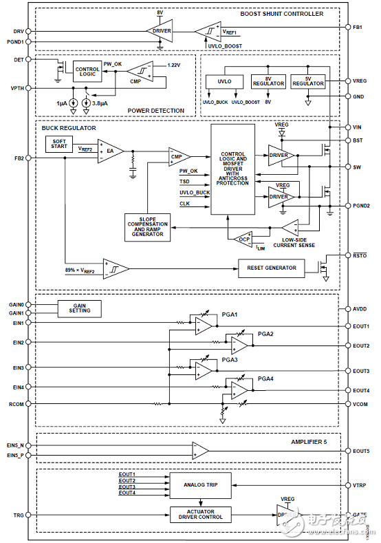
圖1.ADP2450功能框圖
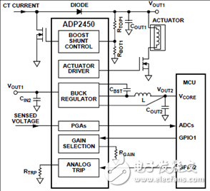
圖2.ADP2450典型應(yīng)用電路圖
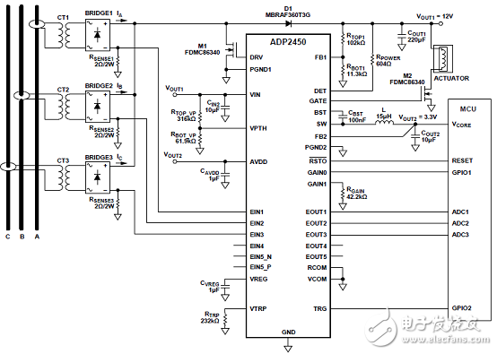
圖3.ADP2450單圈三相檢測(cè)設(shè)計(jì)案例電路圖
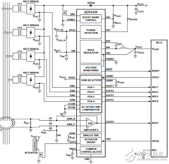
圖4.ADP2450單圈,信號(hào)和電源共享同一CT的應(yīng)用電路圖
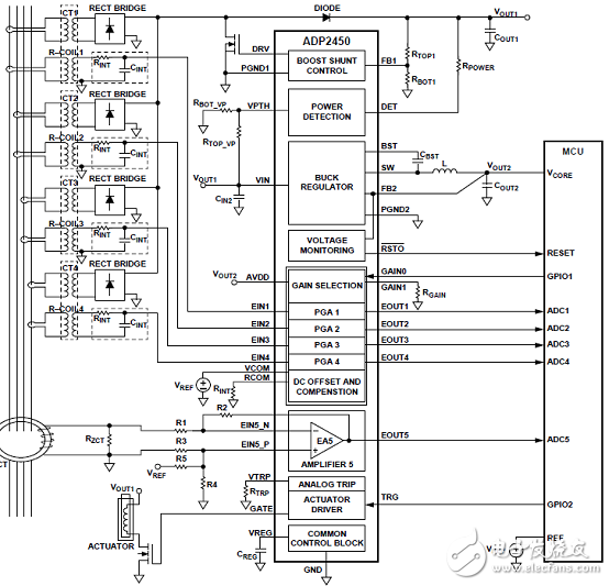
圖5.ADP2450雙圈,CT提供電源和Rogowski(洛氏線圈)提供信號(hào)的應(yīng)用電路圖
評(píng)估板ADP2450ACPZ-3-EVBZ
The ADP2450ACPZ-3-EVBZ evaluation board provides a complete and compact solution that allows users to evaluate the performance of the ADP2450 with a near ideal printed circuit board (PCB) layout. The evaluation board is compatible with current transformer (CT) or ac current source as its input power source. The main device on the evaluation board, the ADP2450, integrates a boost shunt controller with power detection, a high efficiency buck regulator, four low offset and low power consumption programmable gain amplifiers (PGAs), a low offset operation amplifier, a fast analog trip circuit, and an actuator driver. With an external microcontroller unit (MCU) connected, the evaluation board is suitable for quick system evaluation of circuit breaker applications. Full details on the ADP2450 are provided in the ADP2450 data sheet, available from Analog Devices, Inc. Consult the data sheet in conjunction with this user guide when working with the ADP2450ACPZ-3-EVBZ.
評(píng)估板ADP2450ACPZ-3-EVBZ主要特性:
Full featured evaluation board for the ADP2450
Compact solution size
4-layer high glass transition temperature (TG) PCB for superior thermal performance
Connections through vertical printed circuit tail pin headers
Compatible with ac current source input or CT input
Supports single coil and dual coil application
Adjustable output for buck regulator
On-board precision reference
On-board PGA gain setting
Supports analog trip function
Supports power detection function
Voltage monitor and reset output
Flexible connection with external MCU
評(píng)估板ADP2450ACPZ-3-EVBZ應(yīng)用:
Full evaluation of ADP2450
EVALUATION KIT CONTENTS
ADP2450ACPZ-3-EVBZ evaluation board
圖6.評(píng)估板ADP2450ACPZ-3-EVBZ外形圖

圖7.評(píng)估板ADP2450ACPZ-3-EVBZ電路圖
評(píng)估板ADP2450ACPZ-3-EVBZ材料清單:
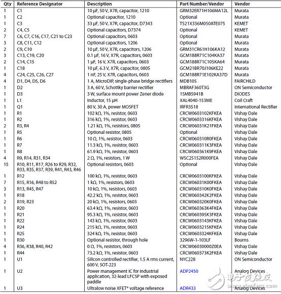
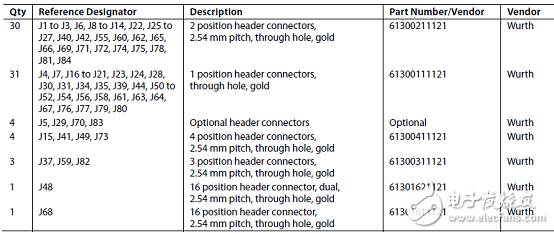
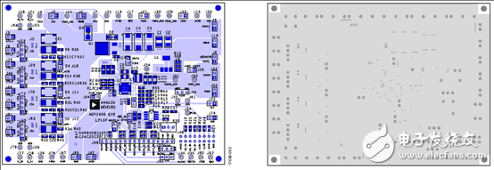
圖8.評(píng)估板ADP2450ACPZ-3-EVBZ PCB設(shè)計(jì)圖:左:元件面;右:層2,地面,
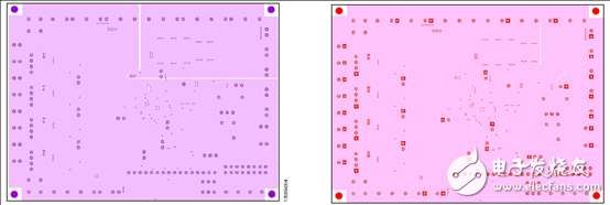
圖9.評(píng)估板ADP2450ACPZ-3-EVBZ PCB設(shè)計(jì)圖:左:層3,電源面;右:層4,底面,
 電子發(fā)燒友App







評(píng)論