Introduction
Flash analog-to-digital converters, also known as parallel ADCs, are the fastest way to convert an analog signal to a digital signal. Flash ADCs are suitable for applications requiring very large bandwidths. However, these converters consume considerable power, have relatively low resolution, and can be quite expensive. This limits them to high-frequency applications that typically cannot be addressed any other way. Typical examples include data acquisition, satellite communication, radar processing, sampling oscilloscopes, and high-density disk drives.This tutorial will discuss flash converters and compare them with other converter types.
Architectural details
Flash ADCs are made by cascading high-speed comparators. Figure 1 shows a typical flash ADC block diagram. For an N-bit converter, the circuit employs 2N-1 comparators. A resistive-divider with 2N resistors provides the reference voltage. The reference voltage for each comparator is one least significant bit (LSB) greater than the reference voltage for the comparator immediately below it. Each comparator produces a 1 when its analog input voltage is higher than the reference voltage applied to it. Otherwise, the comparator output is 0. Thus, if the analog input is between VX4 and VX5, comparators X1 through X4 produce 1s and the remaining comparators produce 0s. The point where the code changes from ones to zeros is the point at which the input signal becomes smaller than the respective comparator reference-voltage levels.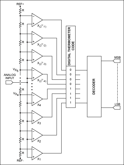
Figure 1. Flash ADC architecture. If the analog input is between VX4 and VX5, comparators X1 through X4 produce 1s and the remaining comparators produce 0s.
This architecture is known as thermometer code encoding. This name is used because the design is similar to a mercury thermometer, in which the mercury column always rises to the appropriate temperature and no mercury is present above that temperature. The thermometer code is then decoded to the appropriate digital output code.
The comparators are typically a cascade of wideband low-gain stages. They are low gain because at high frequencies it is difficult to obtain both wide bandwidth and high gain. The comparators are designed for low-voltage offset, so that the input offset of each comparator is smaller than an LSB of the ADC. Otherwise, the comparator's offset could falsely trip the comparator, resulting in a digital output code that is not representative of a thermometer code. A regenerative latch at each comparator output stores the result. The latch has positive feedback, so that the end state is forced to either a 1 or a 0.
Given these basics, some adjustments are needed to optimize the flash converter architecture.
Sparkle codes
Normally, the comparator outputs will be a thermometer code, such as 00011111. Errors can cause an output like 00010111, meaning that there is a spurious zero in the result. This out-of-sequence 0 is called a sparkle, which is caused by imperfect input settling or comparator timing mismatch. The magnitude of the error can be quite large. Modern converters like the MAX109/MAX104 employ an input track-and-hold in front of the ADC along with an encoding technique that suppresses sparkle codes.Metastability
When the digital output from a comparator is ambiguous (neither a 1 nor a 0), the output is defined as metastable. Metastability can be reduced by allowing more time for regeneration. Gray-code encoding, which allows only 1 bit in the output to change at a time, can greatly improve metastability. . Thus, the comparator outputs are first converted to gray-code encoding and then later decoded to binary, if desired.Another problem occurs when a metastable output drives two distinct circuits. It is possible for one circuit to declare the input a 1, while the other circuit thinks that it is a 0. This can create major errors. To avoid this conflict, only one circuit should sense a potentially mestatable output.
Input signal-frequency dependence
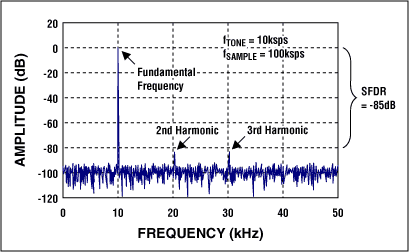
When the input signal changes before all the comparators have completed their tasks, the ADC's performance is adversely impacted. The most serious impact is a drop-off in signal-to-noise ratio (SNR) plus distortion (SINAD) as the frequency of the analog input frequency increases.Measuring spurious-free dynamic range (SFDR) is another good way to observe converter performance. The "effective bits" achieved by the ADC is a function of input frequency; it can be improved by adding a track-and-hold (T/H) circuit in front of the ADC. The T/H circuit allows dramatic improvement, especially when input frequencies approach the Nyquist frequency, as shown in Figure 2 (taken from the MAX104 data sheet). Parts without T/H show a significant drop-off in SFDR.
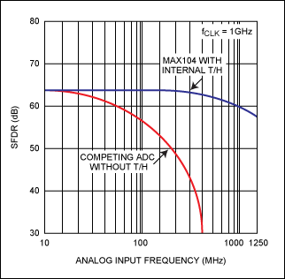
Figure 2. Spurious-free dynamic range as a function of input frequency.
Clock jitter
SNR is degraded when there is jitter in the sampling clock. This becomes noticeable for high analog-input frequencies. To achieve accurate results, it is critical to provide the ADC with a low-jitter, sampling clock source.Architectural trade-offs
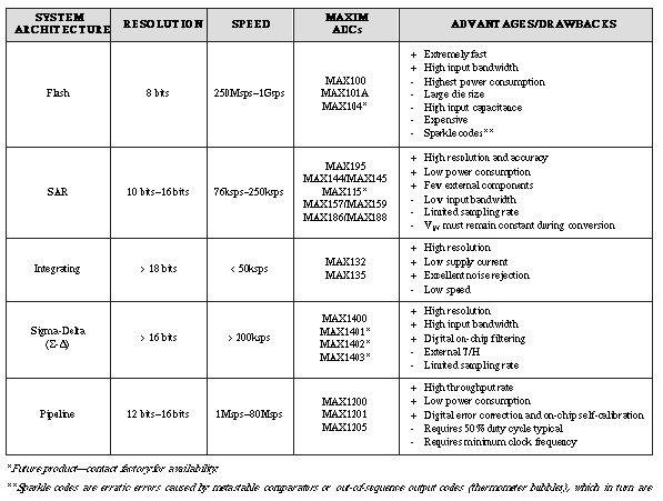
ADCs can be implemented by employing a variety of architectures. The principal trade-offs among these alternatives are:- The time it takes to complete a conversion (conversion time). For flash converters, the conversion time does not change materially with increased resolution. The conversion time for successive approximation register (SAR) or pipelined converters, however, increases approximately linearly with an increase in resolution (Figure 3a). For integrating ADCs, the conversion time doubles with every bit increase in resolution.
- Component matching requirements in the circuit. Flash ADC component matching typically limits resolution to around 8 bits. Calibration and trimming are sometimes used to improve the matching available on chip. Component matching requirements double with every bit increase in resolution. This pattern applies to flash, successive approximation, or pipelined converters, but not to integrating converters. For integrating converters, component matching does not materially increase with an increase in resolution (Figure 3b).
- Die size, cost, and power. For flash converters, every bit increase in resolution almost doubles the size of the ADC core circuitry. The power also doubles. In contrast, a SAR, pipelined, or sigma-delta ADC die size will increase linearly with an increase in resolution; an integrating converter core die size will not materially change with an increase in resolution (Figure 3c). Finally, it is well known that an increase in die size increases cost.
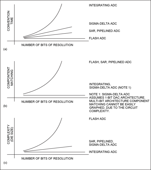
Figure 3. Architectural trade-offs.
Flash ADC vs. other ADC architectures
Flash vs. SAR ADCs
In a SAR converter, a single high-speed, high-accuracy comparator determines the bits, one bit at a time (from the MSB down to the LSB). This is done by comparing the analog input with a DAC whose output is updated by previously decided bits and thus successively approximates the analog input. This serial nature of the SAR limits its speed to no more than a few mega-samples per second (Msps), while flash ADCs exceed giga-samples per second (Gsps) conversion rates.SAR converters are available in resolutions up to 16 bits. An example of such a device is the MAX1132. Flash ADCs are typically limited to around 8 bits. The slower speed also allows the SAR ADC to be much lower in power. For example, the MAX1106, an 8-bit SAR converter, uses 100μA at 3.3V with a conversion rate of 25ksps. The MAX104 dissipates 5.25W, about 16,000 times higher power consumption than the MAX1106 and 40,000 times faster in terms of its maximum sampling rate.
The SAR architecture is also less expensive. The MAX1106 at 1k volumes sells at something over a dollar (U.S.), while the MAX104 sells at several hundred dollars (U.S.). Package sizes are larger for flash converters. In addition to a larger die size requiring a larger package, the package needs to dissipate considerable power and needs many pins for power and ground signal integrity. The package size of the MAX104 is more than 50 times larger than the MAX1106.
Flash vs. pipelined ADCs
A pipelined ADC employs a parallel structure in which each stage works on one to a few bits of successive samples concurrently. This design improves speed at the expense of power and latency, but each pipelined stage is much slower than a flash section. The pipelined ADC requires accurate amplification in the DACs and interstage amplifiers, and these stages have to settle to the desired linearity level. By contrast, in a flash ADC the comparator only needs to be low offset and to resolve its inputs to a digital level; there is no linear settling time involved. Some flash converters require preamplifers to drive the comparators. Gain linearity needs to be specified carefully.Pipelined converters convert at speeds of around 100Msps at 8- to 14-bit resolutions. An example of a pipelined converter is the MAX1449, a 105MHz, 10-bit ADC. For a given resolution, pipelined ADCs are around 10 times slower than flash converters of similar resolution. Pipelined converters are possibly the optimal architecture for ADCs that need to sample at rates up to around 100Msps with resolution at 10 bits and above. For resolutions up to 10 bits and conversion rates above a few hundred Msps, flash ADCs dominate.
Interestingly, there are some situations where flash ADCs are hidden inside a converter employing another architecture to increase its speed. This is the case, for example, in the MAX1200; a 16-bit pipelined ADC that includes an internal 5-bit flash ADC.
Flash vs. integrating ADCs
Single, dual, and multislope ADCs achieve high resolutions of 16 bits or more, are relatively inexpensive, and dissipate materially less power. These devices support very low conversion rates, typically less than a few hundred samples per second. Most applications are for monitoring DC signals in the instrumentation and industrial markets. This architecture competes with sigma-delta converters.Flash vs. sigma-delta ADCs
Flash ADCs do not compete with a sigma-delta architecture because currently the achievable conversion rates differ by up to two orders of magnitude. The sigma-delta architecture is suitable for applications with much lower bandwidth, typically less than 1MHz, and with resolutions in the 12- to 24-bit range. Sigma-delta converters are capable of the highest resolution possible in ADCs. They require simpler anti-alias filters (if needed) to bandlimit the signal prior to conversion.Sigma-delta ADCs trade speed for resolution by oversampling, followed by filtering to reduce noise. However, these devices are not always efficient for multichannel applications. This architecture can be implemented by using sampled data filters, also known as modulators, or continuous-time filters. For higher frequency conversion rates the continuous-time architecture is potentially capable of reaching conversion rates in the hundreds of Msps range with low resolution of 6 to 8 bits. This approach is still in the early research and development stage and offers competition to flash alternatives in the lower conversion rate range.
Another interesting use of a flash ADC is as a building block inside a sigma-delta circuit to increase the conversion rate of the ADC.
Subranging ADCs
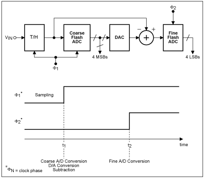
When higher resolution converters or smaller die size and power for a given resolution are needed, multistage conversion is employed. This architecture is known as a subranging converter, also sometimes referred to as a multistep or half-flash converter. This approach combines ideas from successive approximation and flash architectures.Subranging ADCs reduce the number of bits to be converted into smaller groups, which are then run through a lower-resolution flash converter. This approach reduces the number of comparators and reduces the logic complexity compared to a flash converter (Figure 4). The trade-off results in a slower conversion speed compared to flash.
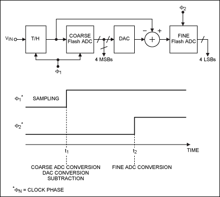
Figure 4. Subranging ADC architecture.
The MAX153 is an 8-bit, 1Msps ADC implemented with a subranging architecture. This circuit employs a two-step technique. First, a conversion is completed with a 4-bit converter. A residue is created, where an 8-bit accurate DAC converts the result of the 4-bit conversion back to an analog signal. The analog signal is subtracted from the input signal. Second, this residue is again converted by the 4-bit ADC and the results of the first and second pass are combined to provide the 8-bit digital output.
Process technology
Flash converter speeds are currently in excess of 1Gsps. The 2.2Gbps MAX109 is fabricated with an advanced SiGE process. The MAX108 (1.5Gsps), MAX104 (1Gsps), and MAX106 (600Msps) 8-bit ADCs are manufactured with Maxim's proprietary, advanced GST-2 bipolar process ("giga"-speed silicon bipolar process).CMOS flash converters are available at lower speed with resolutions compared to bipolar technology offerings. These ADCs are typically intended for integration into a larger CMOS circuit. CMOS, BiCMOS, and bipolar technologies will continue to improve, yielding increasingly higher conversion rates.
 電子發(fā)燒友App





























評(píng)論