Output overvoltage protection is a critical feature for DC-DC converters in order to protect sensitive loads from permanent damage. The basic requirements for an overvoltage protection (OVP) circuit are precise sensing of the output voltage condition and fast activation of the shutdown circuit.
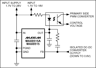
The MAX8515 shunt regulators are excellent candidates for implementing this function in DC-DC converters. These devices offer the advantages of combining an accurate 0.6V reference, comparator and an output drive stage in space saving SC70 and THIN SOT23 packages (Figure 1).
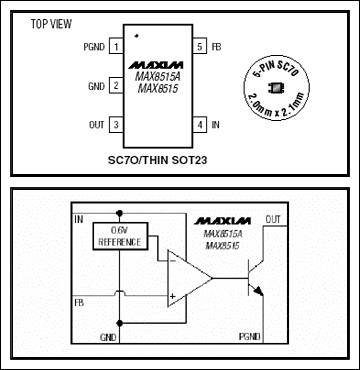
Figure 1.
The salient features of the MAX8515 ICs for the output overvoltage detection application are:
- 0.6V ±1% initial accuracy at +25°C
- 0.6V ±1.8% accuracy from -40°C to +85°C
- Output stage sink capability of 20mA at 0.2V
- Input voltage range from 1.7V to 28V
- Capability to directly drive optocouplers
- Space-saving 5-Pin SC70 or SOT23 packages
- Excellent dv/dt immunity when powered by secondary side bias windings in low output voltage DC-DC converter designs.
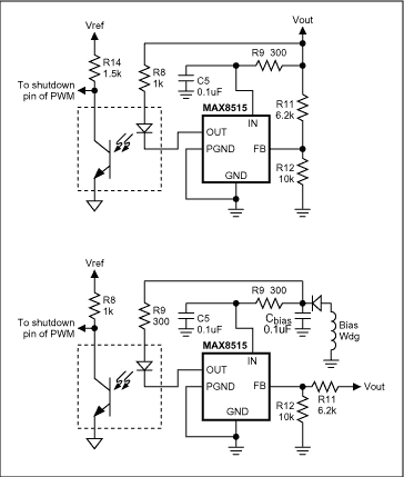
Figure 2. OVP circuit using MAX8515 powered from output voltage of DC-DC converter.
For a lower output stage voltage drop, it is possible to operate the OVP circuit reliably in lower output voltage supplies. Specifically, when compared to other available devices that have an output saturation voltage drop of 1.2 volts, the MAX8515 devices have an output stage drop of 0.2 volts @ 20mA current. This enables the MAX8515 based OVP circuit to operate from power supply outputs lower than competing devices. As shown Figure 3 below, the MAX8515 will sense an overvoltage event down to 1.8 volts whereas competing devices can only sense overvoltage events of 2.7 volts or more.
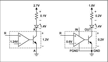
Figure 3. Lower Output stage voltage drop for MAX 8515 extends OVP circuit operation down to 1.5 volt output supplies.
The ability to operate from the smooth, monotonic, low dv/dt output voltage waveform down to output voltages as low as 1.5 Volts eliminates spurious OVP sensing events at startup and provides for a rugged OVP circuit. In supplies with output voltages lower than 1.5 volts, there is not enough voltage headroom the bias the LED, current limit resistor and output stage of MAX8515. Hence it is necessary to use the bias winding approach to provide enough headroom. The output voltage of the peak rectified bias winding however exhibits a significantly higher dv/dt than the DC-DC converter output voltage waveform and therefore presents startup problems. To illustrate the dv/dt issue, consider the waveform of Figure 4. With the 'R' pin of the competing part grounded, a triangle waveform is applied to the Vsupply point.
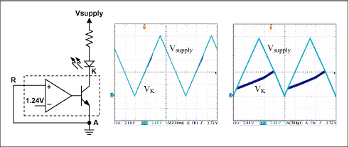
Figure 4. Spurious OVP sensing due to poor dv/dt immunity in industry standard device.
At lower slew rates the, Voltage at the 'K' point and the supply voltage track each other. At higher slew rates typical of secondary bias windings however, the Voltage at the 'K' point fails to track the supply voltage. This causes a voltage difference across the opto LED and the current limiting resistor sufficient to trigger the primary side shutdown circuit, thus preventing the DC-DC converter start up. Additional circuit modifications are required to make the circuit immune to dv/dt. These methods rely on techniques such as diverting a part of the opto LED current with a shunt resistor across the opto LED. The MAX8515 devices are provided with a supply voltage pin that is independent of the output pin, thus providing a reliable means to achieve excellent dv/dt immunity. A suitable R-C delay on the IN (Supply voltage) pin makes the device work reliably at dv/dt higher than 1V/μS, as shown in Figure 5.
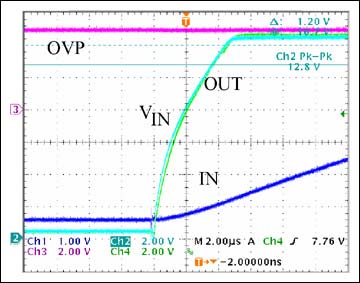
Figure 5. Excellent dv/dt immunity for MAX8515 prevents spurious OVP circuit triggering.
It should be noted that the R-C delay introduced to prevent dv/dt effects does not affect the speed at which OVP events are sensed to any significant level. To illustrate this issue, the performance of the MAX8515 OVP circuit during a Hiccup type OVP event is presented in Figure 6. The FB pin is biased at 0.7 volts and the supply voltage to the MAX8515 is ramped up. It is seen that the OUT pin of the MAX8515 goes down in 10us. This is possible in spite of the introduced R-C delay due to the ability of MAX8515 to operate from a supply voltage of 1.7 volts minimum (guaranteed). It is expected that the output voltage of the DC-DC converter will not exceed its OVP setpoint within 10uS, which is a reasonable assumption considering typical soft start periods employed in DC-DC converters.
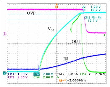
Figure 6. Performance of MAX8515 under hiccup OVP conditions shows only 10μS sensing delay.
Summary: The various issues involved in OVP circuit design for DC-DC converters were presented, and the superior performance of the MAX8515 ICs in this application was demonstrated. The dv/dt issue can be altogether avoided in supplies with output voltages down to 1.5 volts. In Applications where the output voltage is insufficient to bias the LED, the bias winding approach can be safely adopted by providing a suitable R-C delay for the supply voltage pin 'IN', of the MAX8515.
Note: For accurate computations of the OPTO LED current limiting resistor, the Output stage may be modeled by the following equation:

 電子發(fā)燒友App










評論