Introduction
Many new advanced industrial applications require an interface between a high-performance data-acquisition system (DAS) and multiple sensors. When this interface requires multichannel highly accurate amplitude and phase information, these industrial applications can take advantage of very high-dynamic-range, simultaneous-sampling, multichannel ADCs like the MAX11040. This application note explains the MAX11040's sigma-delta architecture and how to select the proper schematic and components to achieve optimal system performance.The benefits of a high-speed, sigma-delta architecture
Consider as an example an advanced 3-phase power-line monitoring/measurement system shown in Figure 1. These industrial applications require accurate simultaneous, multichannel measurement over a wide dynamic range up to 117dB at a sample rate up to 64ksps. To optimize system precision, signals from the sensors (e.g., the CT and PT transformers in Figure 1) should be properly "conditioned" to meet the ADCs input ranges and ensure that the DAS characteristics will enable measurements in compliance with international standards.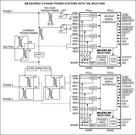
Figure 1. A power-grid monitoring application for a MAX11040-based DAS.
Figure 1 illustrates that two MAX11040 ADCs can simultaneously measure the three phases and a neutral voltages plus the currents. The ADCs are based on the sigma-delta architecture, which uses an oversampling/averaging process to achieve high resolution. Each ADC channel performs analog-to-digital conversion on its input using a dedicated switched-capacitor sigma-delta modulator. The modulator converts the input signal into low-resolution digital data for which the average value represents the digitized signal information at 3.072Msps for a 24.576MHz clock. This data stream is then presented to an internal digital filter for processing to remove any high-frequency noise. The result of these operations is a high-resolution, 24-bit output data stream.
The MAX11040 is also a 4-channel simultaneous-sampling ADC where output data represent processed and averaged values. These values cannot be considered "instantaneous" like in the successive-approximation-register (SAR) ADCs.1,2
The MAX11040 provides designers with many capabilities that are not achievable in a SAR-based architecture: a very high dynamic range of 117dB SNR at 1ksps; integral and differential nonlinearity (INL and DNL) an the order of magnitude better than in a SAR-based ADC; and a unique, adjustable sampling phase (sampling point) that enables internal compensation for phase shift due to external circuitry such as dividers, transformers, or filters at the inputs.
Additionally, the MAX11040 integrates an on-chip digital lowpass filter that processes the data stream from each modulator and generates noise-free high-resolution output data. The lowpass filter has a complex frequency-response function determined by the programmable output data rate. The combination of the input resistor/capacitor (RC) filter and the digital lowpass MAX11040 filter can be used to reduce, or eliminate completely, the complexity of the anti-aliasing filter design required on the input signal path to the MAX11040. Some characteristics of the MAX11040 are shown in Table 1. For more detailed information about the MAX11040's digital lowpass filter or the characteristics shown in the table, see the device's data sheet.
Table 1. Important typical characteristics of the MAX11040 ADC.
| Part | Channels | Input range (VP-P) | Resolution (Bits) | Speed (ksps, max) | SINAD (1ksps) (dB) | Input impedance |
| MAX11040 | 4 | ±2.2 | 24 | 64 | 117 | High, (130kΩ, approx) |
ADC performance requirements in the powerline application
The outputs of the CT (current) and PT (voltage) sensor transformers in this application are typically ±10V or ±5V peak to peak (VP-P). The MAX11040's ±2.2VP-P input range is below these typical outputs from the CT and PT transformers. There is, however, a simple and cost-effective approach to accommodate the transformers' ±5V or ±10V ranges with the MAX11040‘s lower input range. This is shown in Figure 2.The circuit connected to channel 1 represents a single-ended design. In this configuration, one side of the transformer is tied to ground and signal conditioning is achieved by one simple resistive-divider and capacitor.
If common-mode noise (noise which is the same to both ADC inputs) represents a serious concern, then a differential design is recommended as shown in the circuit connected to channel 4. By taking advantage of the MAX11040's truly differential inputs in this design, noise effects are reduced.
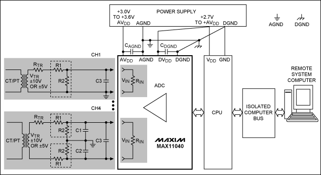
Figure 2. Board-level block diagram of a typical power-line monitoring application using the MAX11040. Drawing shows a ±10V or ±5V transformer interface. The CH4 interface represents a differential design, while the CH1 interface is a single-ended design.
PT and CT measurement transformers represent relatively low-impedance sensors. (Effective impedance, RTR, is in the order of 10Ω to 100Ω). Two assumptions are made for the calculation examples and experiments below: the transformers represent voltage sources with an effective output resistive impedance RTR = 50Ω; and for the purpose of demonstration, the transformers could be replaced by low-distortion function generators with an output impedance of 50Ω, as shown in Figure 3. The input impedance of the MAX11040 is set by the clock rate and ADC input capacitor value. With a proper bypass capacitor, C3, and with XIN clock frequency = 24.576MHz, then the input impedance, RIN, is equivalent to 130kΩ ±15%. The tolerance limits are set by variations in the internal input capacitor.
The resistor-divider networks of R1 and R2 need to scale the input signal ±10V or ±5V to the full-scale range (FSR) of the ADC equaling ±2.2V. For this circuit to work properly, optimal values for the resistors R1 and R2 and capacitors C1, C2, and C3 are selected to accommodate the ±10V or ±5V input values. The resistors R1 and R2 must have a high enough impedance to avoid substantial loading on the CT and PT transformers' outputs. The value of R2 should also be low enough not to be "loaded" itself by the input impedance of the ADC (R2 << RIN).
For single-ended designs, the MAX11040's input voltage, VIN (f), for channel 1 in Figure 2 can be calculated using Equation 1:
Where:
(Eq. 1)
VTR is the output voltage of the CT and PT transformers.
RTR is the transformers' effective impedance.
R1, R2 are the resistive-divider networks.
RIN is the input impedance of the MAX11040.
R2llRIN is the parallel impedance of R2 and RIN. C3 is the input bypass capacitor.
f is the input signal frequency.
VIN(f) is the MAX11040's input voltage.
A very similar approach can be used for a differential design.
To maintain a precision resistance ratio and proper bypass characteristics, resistors should be metal-film type with tolerances of 1% or better and with a low temperature coefficient. Capacitors should be precision ceramic or film capacitors. It is preferable to acquire components from reputable sources like Panasonic?, Rohm?, Vishay?, Kemet?, and AVX? products.
The MAX11040EVKIT offers a fully functional 8-channel DAS. The EV kit can help a design engineer to expedite real-life developments such as verification of the schematic solution suggested in Figure 2.
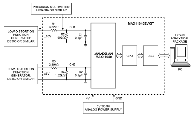
Figure 3. Block diagram of a MAX11040EVKIT-based development system. Two precision instruments are needed to accomplish proper calibration of the measurement channels. Measurement results could be transferred though the USB port to a PC and then converted to Excel? files for further processing.
±5V signals from a function generator are connected to the MAX11040's channel 2, while ±10V signals from a function generator are connected to the MAX11040's input, channel 1. The resistor-dividers networks, R1/R2 and R3/R4 will scale the input signal ±5V or ±10V, respectively, to the approximate full-scale range (FSR = ±2.2VP-P) of the ADC.
Resistor-divider values R1 and R2, as well as the bypass capacitors C1 and C2 shown in Table 2 were selected using equation 1 to achieve a near-optimal input dynamic range (around ±2.10VP-P). This dynamic range is within the limits of the high relative accuracy on the order 0.05%, or better, for the MAX11040. For more detailed information regarding this accuracy specification, see the MAX11040 data sheet.
Table 2. Calculation for resistors and bypass capacitors in Figure 3.
| VTR ±VP-P |
RTR (Ω) |
R1 (Ω) |
R2 (Ω) |
RIN (Ω) |
C3 (μF) |
f (Hz) |
VIN ±VP-P |
VADC (VRMS) |
Calibration Factor-KCAL |
Calibration Factor error (%) |
| Calculations for nominal VTR and standard components (nominal) values | ||||||||||
| 10 | 50 | 3320 | 909 | 130000 | 0.1 | 50 | 2.11268 | 1.4939 | 4.73301 | 0.70 |
| 5 | 50 | 2490 | 1820 | 130000 | 0.1 | 50 | 2.07026 | 1.46395 | 2.41516 | 0.99 |
| Measured values for VTR, VIN, VINRMS with real components values and tolerances used in the experiment | ||||||||||
| 9.863 | 50 ± 10% | 3320 ± 1% | 909 ± 1% | 130000 ± 15% | 0.1 ± 10% | 50 | 2.09872 | 1.483899 | 4.699912 | 0 |
| 4.932 | 50 ± 10% | 2490 ± 1% | 1820 ± 1% | 130000 ± 15% | 0.1 ± 10% | 50 | 2.06151 | 1.45833 | 2.3914 | 0 |
| 0 | 50 ± 10% | 2490 ± 1% | 1820 ± 1% | 130000 ± 15% | 0.1 ± 10% | 50 | 0 | 0.00048 | NA | NA |
The calculations in Table 2 were made with equation 1 and the precision measurements defined for Figure 3. The top portion of the table shows both the theoretical calculations from Equation 1 for nominal input voltages, and the nominal selected standard values for discrete components. The lower portion of Table 2 demonstrates the real component values and tolerances used in the experiment, as well as the measured values used for the FSR calibration and KCAL factor calculations below:
The calibration factor, KCAL, is calculated using Equation 2:
Where:
KCAL = VTRMAX/(VADCMAX - VADC0) (Eq. 2)
VTRMAX is the maximum values of inputs representing signals ±5V or ±10V, respectively.
VADCMAX is the measured and processed ADC values with the MAX11040EVKIT settings similar to Figure 3 and the input signal set to VTRMAX.
VADC0 is the measured and processed ADC values with the MAX11040EVKIT settings similar to the Figure 3 input signal which is set to VIN = 0 (system zero offset measurements).
KCAL (in this experiment) is the calibration factor for the particular channel that will be used for calculation of the input signal VTR using VADC.
The KCAL error calculation shows that the "theoretical" KCAL based on the nominal values only could produce errors in the order of 1% versus a calculation for KCAL based on the real measured values.
These results mean that that a theoretical calculation alone is not sufficient for practical measurement; full-scale calibration (FSR) is needed for each measurement channel if the design is to exceed the required 0.2% precision for energy metering equipment as mandated by the popular EU IEC 62053 standard.
Table 3 shows the results that verify the measurements of the ? FSR input signals. Data were gathered using a precision HP3458A multimeter; ADC measurements and calculations were made with the calibration factor, KCAL, of Equation 2.
Table 3. Verified measurements for ? FSR input signals.
| Generator | Generator | MAX11040 | Calculation | Verr | Requirements |
| Nominal signal (? FSR) | VTR_m - Signal Measured by HP3458A | VIN Measured by ADC | VTR_C = VIN × KCAL | (VTR_M - VTR_C) × (100/VTR_C) | IEC 62053 |
| (VP-P) | (VRMS) | (VRMS) | (VRMS) | (%) | (%) |
| Channel 1: ±5.000 | 3.4892 | 0.74259 | 3.490126 | -0.026544 | 0.2 |
| Channel 2: ±2.500 | 1.7471 | 0.7307 | 1.747384 | -0.016265 | 0.2 |
In Table 3 VTR_M represents the measured value of the input ? FSR signal while VTR_C represents the processed and calculated value of the input signal using the MAX11040's measurements and KCAL.
Results confirm that the measured error, VERR, of the conditioned circuits is below 0.03% which comfortably meets the 0.2% precision requirement mandated by the EU standard IEC 62053.
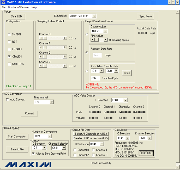
Figure 4. The MAX11040EVKIT GUI allows a user to conveniently set various measurement conditions: 12.8ksps, 256 samples/cycle, and 1024 as the number of conversions. Additionally, the calculation section of the GUI provides a convenient tool for engineering fast evaluations.
For more detailed analyses, measurement results can be transferred though a USB port to a PC and then the powerful (and free) complementary Excel analytical package can be used.
Conclusion
High-performance simultaneous-sampling, multichannel, sigma-delta ADCs like the MAX11040 are especially useful in a new DAS for industrial applications. These new ADCs provide a very high dynamic range up to 117dB, improved integral and differential nonlinearity, and a sample rate up to 64ksps. With a properly selected signal-conditioning circuit, the MAX11040 can meet and exceed the requirements of advanced specifications for "smart" power-grid monitoring systems.1References
- See Maxim's application note 4595, "Reduce system cost for advanced powerline monitoring by leveraging high-performance, simultaneous-sampling ADCs."
- See Maxim's application note 4639, "Signal conditioning in industrial multichannel data acquisition systems (DAS) utilizing high-performance simultaneous-sampling ADCs."
- See Maxim's application note 4272, "Overview of the MAX11040 24-bit simultaneous-sampling, sigma-delta ADC."
AVX is a registered trademark of AVX Corporation.
Excel is a registered trademark of Microsoft Corporation.
Kemet is a registered trademark of KRC Trade Corporation.
Panasonic is a registered trademark of Matsushita Electric Industrial Co., Ltd.
ROHM is a registered trademark of ROHM Co., Ltd.
Vishay is a registered trademark of Vishay Intertechnology, Inc.
 電子發(fā)燒友App





評(píng)論